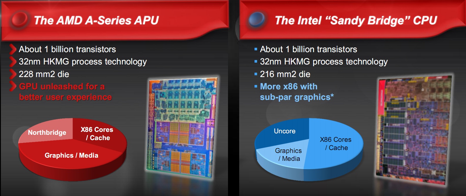
In this article we present a detailed description of the new APU from AMD, whose code name is Llano. We will unveil the details of the system architecture and of the various components integrated into the chip. We will perform also a comparison with the previous architecture, comparing an A8-3850 with a Phenom II x4 840 and a Phenom II 945.
Overview
The Lynx platform is the platform designated by AMD for the mainstream desktop market.
The target audience are the low-power desktop, like the HTPC, All-in-One desktop and dedicated desktop systems for office use, casual gaming and browsing.
The key component is the Llano APU.
After showing the performance and features of the Lynx platform and in particular of the A8-3850 CPU (VERSIONE ITALIANA), in the following pages we will perform a thorough analysis of the architecture and components of the Llano APU, starting with the CPU cores that compose it, including a performance comparison against the previous Stars architecutre, namely Propus and Deneb, concluding with an analysis of the integrated GPU and Northbridge.
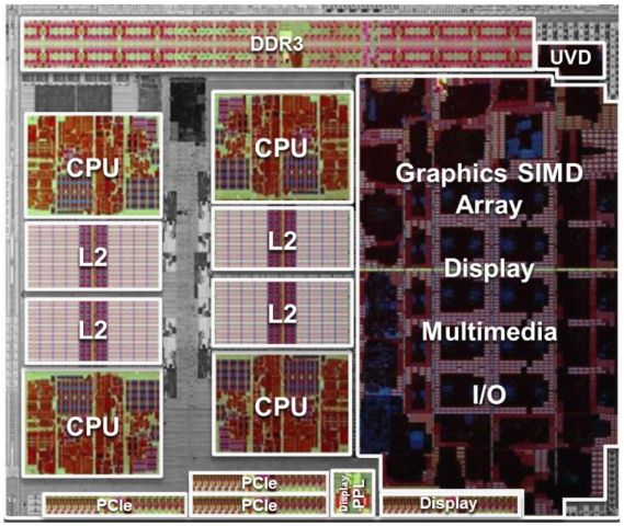
In the first picture you can see a simplified block diagram of the Llano chip. In the second picture you can see a photo of the Llano die.
The heart of the APU are a number of CPU cores, each with its own L1 and L2 caches.
Equally important is the GPU, of DirectX11 class, with an adjacent third-generation UVD unit.
As for external connections we have a memory controller (MC) capable of supporting dual channel DDR3 with 1866 transfers per second, 64 bits each, and the GIO module, which includes the PCI Express 2.0 bus of 24 lines for the connection of both an additional video card or additional displays, both for the implementation of the Unified Media Interface to connect to the Fusion Controller Hub (FCH), and to implement 4 PCI Express link, to avoid encumbering the FCH, and finally the HDMI, DVI and Display Port video links.
The switching center of all data is the north bridge (NB), which is responsible for traffic routing between all the components mentioned above.
The icing on the cake is TurboCore 2.0 technology, which performs a dynamic overclocking of the CPU (and in future architectures also of the GPU), depending on the actual workload of each element.
CPU
The core architecture of the Llano resumes and improves the one of the "Stars" core, with some improvements visible even from the block diagram.
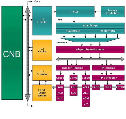
The green block, contains the North Bridge, the I/O controller for the chip and the RAM controller and is shown in the figure, with label CNB. It will be described later.
The gray BUS that you see on the side of the CNB is the only bus onto which all the core comunicate and on which they are enabled to communicate, in turn, by the NB.
The rest of the diagram includes a core and its caches.
Power Saving Techniques
From the description that follows in subsequent pages, for those who already know the previous Stars architecture, it would seem that not much has changed. Actually in the Llano core has been implemented a wide range of advanced energy saving techniques.
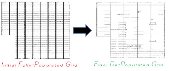
First, the grid that distributes the clock has been completely redesigned and made sparse, ie those branches which were eliminated did not carry the signal to any unit. Then the clock gating was implemented in the various units and with a very high granularity.
The clock gating consists in shutting down clock at parts of a chip to drastically reduce consumption.
Finally, the CC6 energy-saving state was introduced which consists in removing the physical power to the entire core, through a ring of about one million transistors around each core.
It was estimated by AMD that energy saving is equal to 16% at full load, 36% at idle and over 90% in the CC6 energy saving state, compared to a Stars core, by normalizing the consumption for the clock, for the production process and for the number of transistors.
This means that if the Llano core had been made with the 45nm manufacturing process and had the same number of transistors of a Stars core, it will consume as indicated. It has been estimated also that normalizing the consumption as mentioned above, on average, a Llano core consumes 25% less.
The differences with the Stars core are impressive, especially in the state of maximum energy saving, that does not exist in the core of the old generation, as a core was taken at idle to 800 or 1000 MHz, reducing but not eliminating power consumption. In particular there was no clock and power gating.
All this was possible thanks to the excellent SOI process that has been further improved, but as we can see, with Llano has been achieved even more, thanks to the introduction of these new technologies.
Such techniques on the clock grid, on the clock and power gating have been extended to the North Bridge and the GPU, which also benefits from the transition to the 32nm HKMG SOI gate first process of Global Foundries.
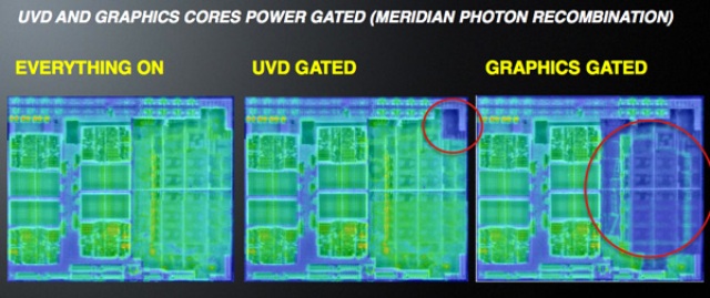
As you can see from the thermal image, the rings of transistors are very effective in reducing heat dissipation. Without them, but only the clock gating, the leakage would remain, being very low in the SOI process, up to 10-20 times less than the competition. But the 32nm HKMG SOI gate first process allows you to use an N-MOS transistor ring, which are able to reduce further the already low leakage by a factor of 10.
Competition instead uses a gate last process, which requires the use of P-MOS transistors, less effective for power gating. Result? The of parts do not almost absorb current, and remain almost at room temperature. A big step forward compared to the Stars core.
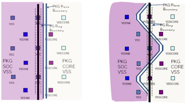
Getting more into energy saving operation, we can say that Llano has two separate supply voltages: VDD and VDDNB. On the first line, all the cores are connected, which then are fed by the same voltage. On the second line the remaining units of the chip are connected: the northbridge, the GPU, the UVD block and the GIO block
Apparently it may seem inefficient to connect all cores at the same voltage, because the VDD must be equal to the maximum voltage required by all cores. But the deep clock gating, the deep power gating, the CC6 state for the cores, the lithography process with a very low leakage and the high efficiency of the N-MOS at the core shutdown allow almost zero consumption for the unused cores.
There are actually two types of C6 power state. The CC6 (Core C6) is the maximum energy saving state of a single core, as we have already seen. But if at least one core is active, the VDD voltage and the clock generator can not be turned off, consuming energy. Here comes the second C6 power state, more profound, called PC6 (Package C6), which engages when all the core have gone in the CC6 state. In this case both the supply voltage and the core clock can be switched off, leading to additional savings.
As for the VDDNB, here a single voltage is a compromise to reduce the complexity of the system, but always with very granular clock gating and power gating, energy savings can be substantial.
As for the core, the VDDNB must be set to the maximum voltage required by the powered components. The northbridge has its own P-states, as well as the GPU, with its memory controller, which is one of the most consuming components of the system and that can be turned off independently of the GPU, the UVD and GIO unit (P-State depends on the speed of PCI Express links, 1.0 or 2.0, which requires higher voltage).
As for the GPU, it can be turned off automatically by the hardware, using a programmable timer from the BIOS or graphics driver itself. But as for the cores, clock gating and power gating, combined with the advanced production process, allows optimum power consumption, as seen in the thermal image above.
Other energy-saving techniques implemented, consist of frame buffer data compression, allowing you to transfer less data and therefore save energy and a technique implemented in the mobile version, called adaptive backlight modulation (ABM), which consists in modulating the brightness of the display backlight lamp according to the displayed content, to reduce energy consumption without affecting the images displayed in a visible way.
Caches Architecture
The Llano cores have an L1 instruction cache, L1 data cache and an unified L2 cache. The L3 cache has been eliminated, compared to some of the Stars core, so the cache structure follows that of the Propus core. This can make you lose a few percentage points in performance, on memory-hungry applications, but as we will see later, the improvements to the core, the L2 cache and the memory controller, combined with faster memory, in many cases compensate for this lack.
The reason for the elimination of the L3 cache is a matter of energy saving, in addition to space saving. The unique architecture of the AMD CPU cache means that when you have to look for a datum, it must be sought in the L3 cache and all other CPU cache. But with the C6 power state, it is possible that they should be made awake, making the process very slow, complicated and expensive. In essence, the implementation of the C6 state would be inefficient with an L3 cache.
Another difference between the Llano and Stars core cache is that the L1 data cache is of 8 transistors type in Llano, compared with 6 of the previous generation. The 8 transistors caches increase, as can be imagined, the space occupied by the cells, but allow for greater speed, more reliability, low voltage and thus lower consumption.
L1 instruction cache
The instruction cache size is 64KB and ti is two-way set associative, with lines of 64 bytes each. This unit is responsible for loading instructions, doing prefetching, pre-decoding, to determine the end of each instruction and the beginning of the other, and keeping the information for the branch prediction.
The data that are not present in the cache are requested to the L2 cache or the system memory. In this case the cache requires two lines of 64-byte naturally aligned and consecutive, so doing a prefetch of possibly successive instruction, since the code typically has spatial locality.
The cache lines are replaced with the LRU algorithm (Least recently used).
During these cache fills, the pre-decoding information, which determine the instruction boundaries, are generated and stored with the instructions in the appropriate bits. This in order to more efficiently decode the instructions in the downstream decoder. The cache is protected only by parity bits.
L1 Data Cache
The data cache size is 64KB and it is two-way set associative, with 64 byte lines each and with two 128-bit ports. It's managed with the write-allocate policy (namely when writing a datum, it is stored in any case in the L1 cache) and write-back policy (namely the data is written physically in the lower levels, such as L2 cache or RAM, only when it should be removed from the cache).
The cache lines are replaced with the LRU algorithm.
It's divided into 8 banks of 16 bytes each. Two accesses in the two ports are possible only if both are aimed at different banks. The cache supports the MOESI coherence protocol (Modified, Owner, Exclusive, Shared, and Invalid), and ECC protection. It has a prefetcher that loads the data in advance to avoid misses and has a 3 clock cycles latency.
L2 Cache
The L2 cache is integrated on-die, proceeds at the same frequency of the CPU and there is one for each core. It is also an exclusive cache architecture: the cache contains only modified lines from the L1 to be written into RAM and that have been designated by LRU algorithm to be deleted from the L1 cache, because it must be replaced with new data. These lines are called victim.
The L2 cache latency is 9 clock cycles in addition to the L1 cache one. In Llano the L2 cache is 1MB 16-way, against 512KB 8-way of most of the Stars core (only dual core Regor has 1MB of cache). The L2 cache is protected with the ECC error protection code.
Translation-Lookaside Buffer
The translation-lookaside buffer (TLB) holds the most recent virtual address translation information used and therefore accelerates its calculation.
Each memory access goes through various stages. The first step is addressing. An instruction specifies an addressing mode which is simply the calculation procedure to find the address (linear also called virtual) of a given data.
There are various methods of addressing. The simplest is the immediate, in which the data is included in the instruction. In this case there is no need to further access to memory. Then there is the direct, in which in the instruction is specified the absolute address of the data. There are other types of addressing (indirect, indexed, with offset, etc. ) and other features of x86-64 architecture (segmentation), which require the calculation, more or less complicated, of the final address (usually done in the AGU, which are described below), but the end result is a linear or virtual address.
If virtual memory is enabled (and in modern operating systems it is always enabled), the virtual address must be translated into a physical address. Here come into play the TLB. The address translation involves the division of the address space in pages of 4KB (even if the CPU supports pages of 4KB, 2MB, 4MB and 1GB), where for each of them security information and physical location of the data is stored.
So for each process there is a table of pages, organized as a tree with multiple levels. For each memory access we should access and navigate the tree, going into the RAM. Without the TLB this would be a very slow process. Instead, the TLB caches the latest information from the translation used.
Llano uses a 2-level TLB structure.
Level 1 instruction TLB
The L1 instruction TLB is fully associative, with space for 32 translations of 4KB pages and 16 for 2MB pages.4MB pages require 2 2MB locations.
Level 1 data TLB
The L1 data TLB is fully associative, with space for 48 translations of 4KB, 2MB, 4MB and 1GB pages.4MB pages require 2 2MB locations.
Level 2 instruction TLB
The L2 instruction TLB is 4-way associative, with space for 512 4KB page translations.
Level 2 data TLB
The L2 data TLB has space for 1024 translations of 4KB pages (compared with 512 of the Stars core: this implies a greater probability of finding the translation in the cache and the ability to handle double the memory for the same performance), 4-way associative, 128 translations of 2MB pages, 2-way associative and 16 translations of 1GB pages, 8-way associative.4MB pages require 2 2MB locations.
Fetch and Decode Unit
The fetch and decode unit performs the translation of the ancient and complex x86-64 instruction set into more manageable macro-ops. Each macro-op is able to describe an arithmetic/logic, integer or floating point, and simultaneously a memory operation, whether read, write, and read-modify-write (atomic operation, useful for implementing semaphores in operating system kernels).
Llano is not very different from its predecessor. It incorporates two separate decoders, one to decode and split simple instructions (up to 2 macro-op), so-called DirectPath, and one for more complex instructions, so-called VectorPath (3 or more macro-op).
When the instruction window (which includes 32 bytes divided into two 16-byte parts) is read from the L1 instruction cache, the bytes are examined to determine if the instructions are of the type DirectPath or VectorPath (this is one of the information that is part the pre-decode and is stored in the L1). The output of these decoders maintains the program order for the instructions.
As we will see later, Llano is an out-of-order architecture, which can execute instructions out of order for faster execution.
These decoders can produce up to three macro-ops per cycle, which can come exclusively from one of the two types of decoders, in each cycle. The output of these decoders are combined and passed to the following unit, the Instruction Control Unit (ICU).
Since the decoding of a VectorPath instruction produces at least 3 macro-op and you can only send to the ICU the macro-ops of one unit at a time, decoding of the VectorPath instructions stops DirectPath instructions decoding. DirectPath instructions that can be decoded in a cycle depends on the complexity of them.
The DirectPath decoder can decode any combination of x86 instruction of DirectPath type that results in a sequence of 2 or 3 macro-op, considering that the decoding is done in program order. So 3 instructions are possible if there are 3 consecutive instructions that give one macro-op, so-called DirectPath Single.2 instructions are possible if one is DirectPath Single and the other is DirectPath Double (so are called the simple instructions that generate two macro-ops). It's possible to decode a single instruction if there are two consecutive DirectPath Double instructions, which can not be decoded together as this would produce 4 macro-ops, beyond the limit of 3 of the architecture.
Another limitation to the amount of decoded instructions is the fact that in a given cycle can be accessed a single block of 16 bytes, of the 32, at a time and then can be decoded only the statements contained in that block. Since there are some instructions that can comprise up to 15 bytes, it is possible that a in block of 16 bytes are not present a sufficient number of instructions to commit all the decoders.
Branch Prediction
The branch prediction in Llano works the same way as the previous generation. A new jump is predicted as not taken until it is actually taken once. Next the jump is predicted taken as long as this prediction is not actually wrong. After these two wrong predictions, the CPU starts to use the Branch Prediction Table (BPT).
The fetch logic accesses the L1 instruction cache and BPT in parallel and the information in the BPT is used to predict the direction of the jump. When the instructions are moved to the L2 cache, the pre-decode information and the jump selectors (which indicate in what condition is the jump, namely never seen, once taken, taken and then not taken) are copied and stored with them instead of the ECC code.
The branch prediction technique is based on a combination of a branch target buffer (BTB) of 2048 elements and a global history counter bimodal (GHBC) of 16384 elements with 2 bits containing a saturation counter used to predict whether a conditional branch should be predicted as taken. This counter contains how many times in the last 4 runs the jump has been taken and therefore the jump is predicted as taken if it has been taken at least 2 times recently.
The GHBC is addressed with a combination of an unspecified number of conditional jump results and the address of the last jump. This is a standard prediction technique that provides the table address with a hash of the jump address combined with the outcome of the last n jumps.
The branch prediction also includes a return address stack (RAS) of 24 items to predict the destinations of procedure calls and procedure returns. Finally, there is a table of 512 elements to predict indirect jumps, even with multiple destinations.
Sideband Stack Optimizer
This unit keeps track of the stack-pointer register. So that can be run in parallel several instructions that require this as the input register (CALL, RET, PUSH, POP, indexing by the stack pointer, calculations that have the stack pointer as a source register).
Instructions that can not be executed in parallel are those that target stack-register, the ones address indexed (in which calculations are made on the register) and the VectorPath instructions that use in some way that register (because of the difficulty to keep track of the register in VectorPath instructions).
Instruction Control Unit
The ICU is the control center of the processor. It controls the centralized register for the executing instructions reordering and the integer and floating point schedulers.
It's responsible for the dispatch (ie the forwarding to the appropriate scheduler) of macro-ops, the retire (ie the determination and validation of the result) of macro-ops, the dependency resolution of registers and flags, by the renaming (a technique to run in parallel unrelated instruction accessing the same register), the management of execution resources, interrupts, exceptions (during the retire of macro-ops) and the management of the incorrect prediction of jumps, which includes emptying the various queues and the cancellation of the ongoing operations.
The ICU takes up to 3 macro-ops per cycle, previously produced by the decoder and places them in a centralized reorder buffer, consisting of 3 lines of 28 macro-ops, which represent an increase over the 24 of the previous Stars architecture. This increase can give rise to more margin to the upstream decoder, because if the downstream instructions are not executed for lack of data from memory, for example, this queue fills up quickly. Increasing it decreases the stall time of the decoder, that must stop if the queue is full.
This buffer allows you to keep track of a maximum of 84 macro-ops, both integer and floating point. The ICU can submit simultaneously macro-ops to the various integer or floating point scheduler, which will make the final decoding and execution of the macro-ops.
Upon completion of the execution, the ICU performs the instruction retire, in program order, and handles any exceptions, including the erroneous prediction of a jump.
It's worth noting that the various macro-ops can be executed out of order and in parallel, both within the same unit (integer or floating point) and when executed on different units. The dispacth and retire do occur, however, in program order.
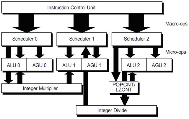
Integer unit
It contains two components, the integer scheduler and integer execution units.
Integer Scheduler
It is based on a 3-way queuing system, also called reservation station (RS) which supplies the three execution units. Each of the 3 queue has room for 10 macro-op (8 in the previous Stars architecture: longer queues mean higher chance of re-ordering of instructions and thus more performance) for a total of 30 manageable macro-ops. Each RS divides the macro-ops in its arithmetic and logical address generation members.
Integer execution units
The integer execution unit (IE) consists of 3 elements (pipeline 0, 1 and 2). Each element is composed of an arithmetic logic unit (ALU) and an address generation unit (AGU). The IE is organized to coincide with the 3 macro-op dispach pipelines of the ICU, as shown in the figure.
The macro-ops are broken into micro-ops in the schedulers. The micro-ops are executed when their operands are available both in the registers or in the result buses: in some interdependent instruction cases, it is not necessary to write the result into a register first and then read it in the next cycle, but you can connect the two instructions with an available result bus.
The micro-ops from a single macro-op can be executed out of order and also a particular integer pipeline can perform micro-ops from various macro-ops (one in the ALU and AGU) simultaneously.
Each of the three ALU is capable of performing logic, arithmetic functions, conditional processing, state flag processing and jump state calculation.
Each of the three AGU is able to calculate the linear address for a memory access or LEA instruction (which calculates the actual address of a datum without going in memory. Indeed LEA stands for Load Effective Address, which calculates and loads the actual address).
It's featured a unit for reads and writes in memory, which actually accesses the L1 data cache, described later (LSU, load and store unit).
The integer scheduler sends a completion signal to the ICU to indicate that a macro-op has been executed. The ICU will retire the instruction when all relevant macro-ops have been executed.
Almost all integer operations can be performed by either of the 3 ALU, with the exception of multiplication, division, LZCNT (leading zero count, ie counting the zeros of a binary number) and POPCNT (population count, ie count of '1' in a binary number).
The multiplications are handled by a pipelined multiplier, which is fed from the pipeline 0. To multiply, however the pipeline 0 and 1 are kept locked simultaneously, since the result of all the multiplication operations in the x86 architecture is double-precision and requires two specific target registers. During execution, the two pipeline 0 and 1 can not be used except for other multiplications (because the multiplier is pipelined). The multiplier of Llano has been further improved compared to previous generation Stars cores.
Similarly, the division uses the pipeline 1 and 2 and the integer divider is fed by pipeline 2, since the division in the x86 architecture starts from double-precision result and gives result and the rest in two separate registers. During the execution the two pipelines 1 and 2 can not be used except for other divisions (because the divisor is pipelined).
In the previous architecture (Stars core) there was not an hardware divider, but the division was a long VectorPath instruction blocking the pipelines 1 and 2 for as long as its long-running (in Llano divisions are also twice as fast) and since there was not a pipelined divider, only a division could be made at a time.
The POPCNT and LZCNT instructions are executed in an unit fed from the pipeline 2 and while it is running one of these instructions, the pipeline 2 is not usable by other instructions other than these two (because the unit is pipelined).
Ultimately a multiplication stops the execution of all non multiplicative instructions in the pipeline 0 and 1 and also of all the divisions, which also require the pipeline 1 to run. The division stops the execution of all non division instructions in the pipeline 1 and 2 and hence the multiplication, requiring the pipeline 1, and LZCNT and POPCNT instructions block all instructions that require the pipeline 2 and therefore also the divisions.
Floating Point Unit
Floating Point Unit (FPU) contains two components, the floating point scheduler and floating point execution units
Floating Point Scheduler
The scheduler is able to accept 3 macro-ops for cycle in any combination of supported instructions: x87 floating-point, 3DNow, MMX, SSE1/2/3/4a.
It manages the register renaming and has a buffer of three lines of 14 elements each, for a total of 42 elements (the previous Stars architecture had 3 queues of 12 elements for a total of 36 macro-ops: here longer queues mean more performance too).
It also runs the superforwarding, which is to forward the results of a read from memory operation to dependent operations at the same clock cycle, without waiting for writing to registers, as is the case for the regular forwarding that normally occurs in this unit and the integer unit, through the use of the result buses.
Also performs micro-ops forwarding and out of order execution. The scheduler communicates also with the ICU to retire the completed instructions, to manage the results of various floating point conversion instructions to integer and vice versa (the two integer and floating point units use a 64 bits bus to communicate) and to receive results nulling commands due to incorrect prediction of a jump.
Floating point execution unit (FPU)
The FPU handles all register operations of x87, 3DNow, MMX and SSE1/2/3/4a instruction sets.
The FPU consists of a stack renaming unit (because x87 does not work with registers but with a stack architecture of 8 elements, inherited from the first external x87 FPU), which allows translating stack access to an 8 registers access, a conventional register renaming unit, a scheduler, a register file, which contains the physical registers and execution units each capable of processing up to 128 bits per clock cycle. The figure shows a block diagram for the flow of data of the FPU.
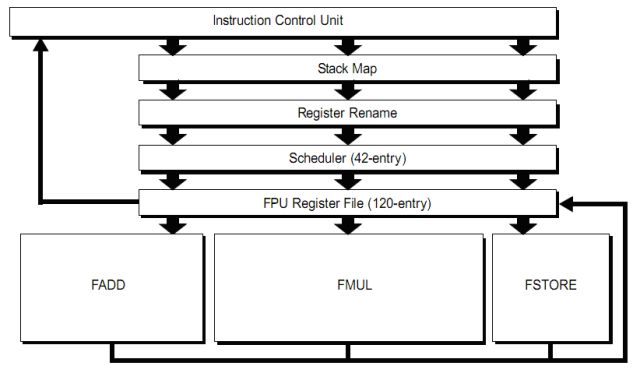
As is shown in Figure the FPU consists of 3 units (FADD, FMUL, and FSTORE).
The FADD unit is able to carry out any instructions of addition and subtraction, both integer SIMD (3DNow!, MMX and SSEn), both floating point, and the types of movement between registers, and shuffle (exchange) and SSEn extract.
The FMUL unit can execute all the instructions of multiplication, division, inverse, square root and transcendental, both integer SIMD (3DNow!, MMX and SSEn), both floating point, and the movement between registers and some simple types of shuffle and extract.
The FSTORE unit is used, alone or in tandem, in each instruction that requires a memory access and is also capable of movement between registers.Load and store unit
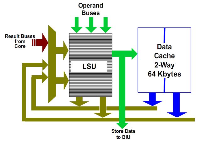
Load-Store Unit, LSU
The L1 data cache, and LSU are shown in figure. L1 data cache supports up to 2 128-bit read operations per cycle or two 64-bit writes per cycle or a mixture of these two.
The LSU has two queues, LS1 of 24 elements and LS2 of 64 elements (12 and 32 in the previous Stars architecture).
The LS1 unit can start two L1 cache operations (reads or tags control for later writing, remembering that the cache uses write allocate policy, then you should check if the data is cached before writing) for each clock cycle. Read operations can start out of order, provided that certain conditions are verified.
The LS2 queue contains requests that have given a miss in the L1 cache after the check made by the LS2 unit. The stores are taken from the LS2 queue, however, then it will have the tag check result.
The 128-bit writes are treated in a special way, since you can write 64 bits at a time, and take up two slots in the LS2.
Finally, the LSU will ensure that the sorting rules of the memory operation of the x86 architecture are observed.
Write Combining
Llano has 4 buffers of 64 bytes (one cache line) and 8 address buffer for merging up to 8 writing to 4 different cache lines.
When multiple stores are executed at a short distance, it can be useful to combine them together before they are written completely, in order to improve the efficiency of writing.
This feature is particularly useful when the data to be written is to external devices that are connected via the PCI Express bus or to the south bridge.
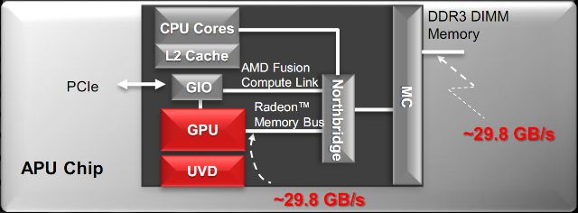
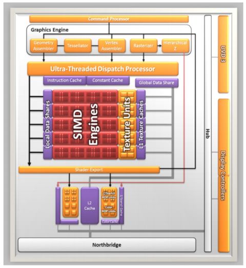
North Bridge, GIO and Memory Controller
In the figure is shown a simplified block diagram of the architecture of the heart of Llano, ie components that track data and manage communication with the outside world: the North Bridge, the GIO unit and the memory controller.
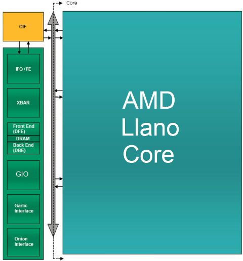
The green block, containing the elements called IFQ/FE, Xbar, Front End (DFE), DRAM, Back End (DBE), GIO, Garlic Interface and Onion Interface, are on the chip north bridge, abbreviated to CNB.
The yellow block, called CIF is a block of synchronization between the CNB and each core, which unifies and directs the flow of data to and from the cores with the CNB. Its task is to implement the CCI interface, Common Core Interface, which is the single point of access to CNB for all cores.
This block is one that implements the algorithm that decides which of the core can speak in a given time and sorts requests from other parts of the chip to the core, such as cache probing, which is performed to see if the core cache has newer data than the RAM.
Now for the building blocks of the CNB.
The IFQ/FE block contains the request queue of the CPU and GPU in the IFQ that is thus an unified queue.
It also includes a logic block, called the Front End (FE) that handles requests for data transfer to and from the cores (which go through the CCI interface), to manage requests to transfer data between the Onion interface and CPU, to handle requests for CPU cache probing by the various components and to maintain the coherence and consistency between the various units.
Xbar block is the so-called crossbar switch, ie the unit that allows the connection between the various units connected to the CNB.
It's basically a digital switch that connects every moment sender and receiver of a communication between the various actors in the system, such as the CCI interface, the controller RAM, Onion and Garlic interfaces, and so on.
DRAM blocks, DBE and DFE are part of the memory controller (MC).
The DFE block, called data front-end, select the requests to send to the rest of the RAM controller and decides between Onion (coherent) , Garlic (not coherent) and CCI (coherent) requests.
Requests are physically carried out by the DBE block, called Data Back End, which synchronizes the CNB with the physical interface to DRAM and sends transfer commands to it.
Garlic interface is a bi-directional, low latency connection, and so it's direct, between the GPU and RAM controller Data Back-end.
When the Data Front End has given the consent, the GPUs can communicate with the controller RAM directly.
Onion interface is a bidirectional connection between the GPU and the IFQ queue. It's used to connect the CPU to the GPU.
The block indicated with GIO (Graphics and I/O) is the block that handles the chip I/O, and is connected to the Xbar unit of the North Bridge (CNB) to communicate with the core and the RAM controller and has a direct and privileged link with the GPU. This is because the controller manages up to 32 PCI Express lines, configurable in many ways.
Four lines are reserved for the UMI interface (Unified Media Interface), which is nothing more than a 4 lines PCI Express link dedicated to the connection with the Fusion Controller Hub (FCH, the south bridge).
Four PCI Express are reserved for various devices, such as sound cards, to not having to impair the FCH and configurable as single lines, double lines, two singles and a double line or a single x4 interface.
Sixteen lines are used for discrete graphics cards, configured in a x16 interface or two x8 interfaces, for CrossFire.
Alternatively, interfaces can be configured as x8 video outputs, in order to use the Eyefinity technology, losing the possibility of CrossFire/DualGraphics.
The remaining 8 lines are used to implement HDMI, DVI and Display Port interfaces.
The gray BUS that you see on the side of the CNB and the CIF is the only bus connection onto which all the core are connected and on which they are enabled to communicate, in turn, from the CIF block.
Integrated RAM Controller
The Llano RAM controller supports dual independent 64-bit channel of DDR3 RAM with 8-bit and 16 bit chip, supporting chip and channel interleaving useful to increase performance by reading consecutive data from several chips in parallel, includes scheduling algorithms for the opening and closing of memory pages, especially optimized for interspersed read and write streams, includes scheduling algorithms to optimize the interspersed data flow from the CPU+Onion and Garlic interfaces and includes an hardware prefetcher.
In particular, the pages used by the GPU accesses are closed immediately, because they generally are streaming accesses, to free pages for CPU accesses, typically more varied.
The data loaded by the prefetcher are maintained in the controller itself and not speculatively sent to L1 and L2 caches.
The prefetcher is able to capture both increasing or decreasing access trends even with non-uniform spacing, using as measure unit the cache line (64 bytes) and is able to detect even separate sequences of accesses. Llano also can keep track of 8 sequences of accesses simultaneously (Stars architecture can keep track of 5 of it).
The Llano memory controller has been greatly improved compared to the Stars cores. It was improved internal efficiency and prefetching algorithms, in particular the Llano core is able to better recognize patterns of memory access, because it is able to associate the actual instruction that accesses memory (IP-based prefetching) and thus is no longer distracted by other instructions in between. In addition, internal buffers have been increased.
The supported RAM frequency was increased up to 1866 MHz (with one DIMM per channel only), compared to the 1333 MHz of the previous generation. On the other hand DDR2 memory, 4-bit chip and ECC correction support was removed, the latter typically used on the server side.
CPU tests: system and testing methodology
Here are the tables containing the technical specifications of the system used to perform the processor tests.
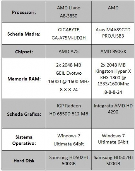
The tests were conducted at default frequency the Phenom II 945, namely 3GHz, and 3016MHz (104MHz for the bus frequency and 29 for the multiplier) for Llano. The Phenom II 840 was downclocked via multiplier to 3GHz (the default frequency is 3.2GHz). The RAM was set to 1600MHz, with 8-8-8-24 latencies for Llano and the Phenom II 840 and to 1333 with 8-8-8-24 latencies for the Phenom II 945.
Following are the software used for CPU testing:
SYNTHETIC
3DMark Vantage: produced by Futuremark, 3Dmark Vantage is a useful tool to test the performance of your system. Primarily designed to track the performance of the graphics card, the 3DMark Vantage is suited for testing of the CPU that are increasingly a bottleneck in the system when it comes to graphics applications. The test was carried out only in relation to the CPU, disabling the 2 steps related only to vga.
PCMark Vantage: Another famous benchmark produced from Futuremark that has the task of analyzing the performance of the entire system. The tests made are CPU-related and include: data encryption, decryption, compression, decompression, image manipulation through the CPU, audio transcoding, video transcoding, and many other tests.
AIDA64: AIDA64 is a software product from FinalWire that monitors the system by providing detailed information on hardware components. The software includes a utility inside the bench capable of testing memory and cache inside the processor.
DATA COMPRESSION AND MULTIMEDIA
7zip 9.20: this well-known archive software contains within it a tool that can analyze system performance, reporting a value expressed in MIPS (million instruction per second). The tests include compression, decompression, and overall value.
Winrar 3 Beta 4: Another famous compression and decompression software for data archives. Inside it there is a benchmark utility that compresses a standard file suitable for this purpose; the software will return the compression speed in KB/s.
Cinebench 11.5 and 10: Software products from Maxon that allow, through the development of three-dimensional images and content, to test the CPU performance. Both the release allow to test the CPU using a single core, or all the cores inside the processor.
X264 HD Benchmark 3.0: software to measure the performance of the CPU using the x264 video encoding.
Handbrake 0.9.5: Multi-threaded video encoding software with which we will transform a file (a movie) to MP4; the process includes x264 video encoding, FAAC audio encoding and muxing into final MP4 container. The time it takes for the CPU to perform this task will be taken into consideration.
Synthetic tests
3DMark Vantage
We begin our tests starting from the benchmark produced by Futuremark, 3DMark Vantage. The test was done by selecting only the two-step related to the CPU and the performance preset setting.
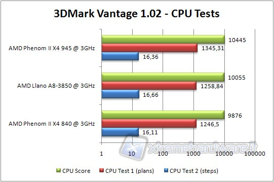
Llano is exactly half way between the Phenom II 840 and the Phenom II 945, as expected. The difference between the CPU test 1 and 2 is probably due to a greater or lesser commitment of the memory, where the L3 cache can make the difference.
PCMark Vantage
We continue with the other benchmark from Futuremark, the PCMark Vantage. In this case we have selected only the PCMark Suite.
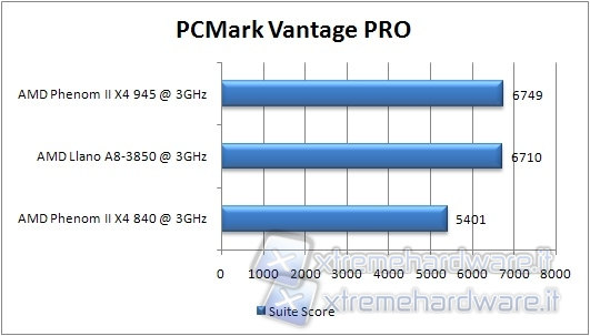
Also in this test Llano goes between the two old-generation CPUs, but this time the L2 cache and the other improvements led him close to the Phenom II 945.
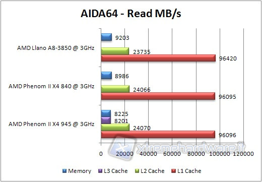
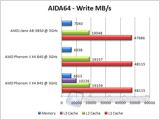
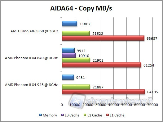
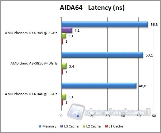
AIDA64 EXTREME ENGINEERING
Moving on to FinalWire software.
We launch the benchmark related to memory and cache, noting that with regard to latency, a lower value equals better performance.
Data compression & Multimedia Test
7zip 9.20
Let's move to the benchmarks related to compression, decompression and multimedia files from a known program to manage archives: 7zip.
Let's launch the tool of performance measurement and verify the values, expressed in MIPS, the software reports.
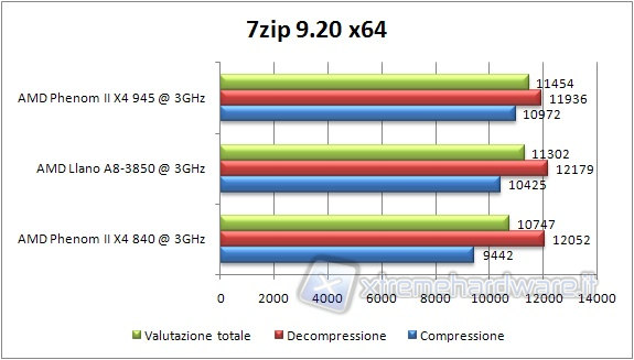
Llano performs half way between the two Phenoms and is surpassed in the compression by Phenom II 945 despite its slower RAM speed. In this case, the L3 cache helps. So much so that the Phenom II 840 is in trouble. As for the decompression, the memory bandwidth here counts more, and then the Llano and the Propus have the upper hand.
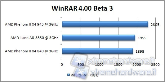
WINRAR 4 Beta 3
The Winrar benchmark consists of the compression of a software predefined file, reporting a value in KB/s.
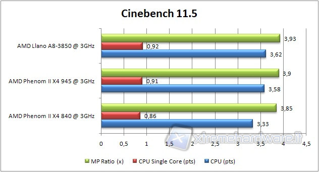
CINEBENCH 11.5
Let's launch Cinebench 11.5, able to test the performance of a CPU by handling and processing of images.
This software, as well as version 10, is highly parallelized and takes full advantage of all processors in the system.
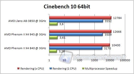
CINEBENCH 10
Also this benchmark uses full multicore technologies.
Let's analyze the recorded data.
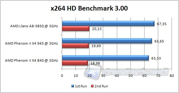
X264 HD BENCHMARK
This benchmark enables the assessment of performance by converting a chosen file in the x264 format.
This operation is carried out in four phases by two steps each.
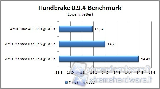
HandBrake
Let's launch Handbrake with the task of transforming a 698MB MP4 movie verifying which processor needs less time to complete the operation; in this case a lower value on the graph indicates a superior performance.
Considerations on CPU tests
In synthetic and compression tests, Llano shows gains against the Propus core, thanks to the various improvements to the core, but loses slightly against the Phenom II 945, due to the lack of L3 cache, as these tests are more dependent on memory, where L3 cache and a lower latency due to the absence of a GPU can make a difference. But Llano excels in multimedia applications, where it is important both to have greater computing power, both to be more effective in prefetching and streaming data to memory, where the enhanced RAM controller does his best. In synthetic tests, however, the data is typically accessed in a more random pattern and quite often reused. So larger cache can result in some advantage.
GPU
The Llano chip GPU component, code-named "Sumo", incorporates many of the characteristics of the AMD "Redwood" GPUs family, which is implemented in the Radeon 5500 and Radeon 5600.
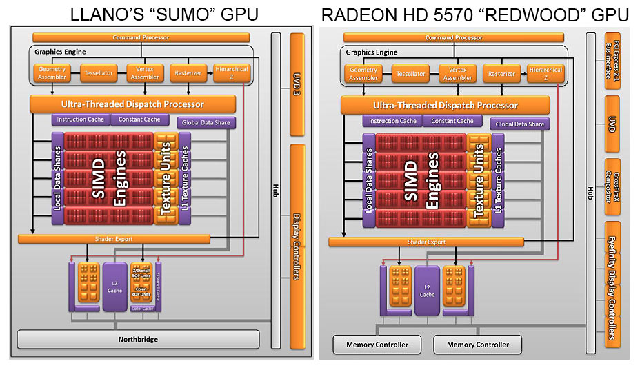
By comparing the two images, we see that not much has changed between "Sumo" and "Redwood" in the computing heart. We have the SIMD engines, 5 in total, each consisting of 16-thread processors and 4 texture units.
Each thread processor consists of a unit with a VLIW 5 architecture, capable of running up to 5 operations per clock cycle, giving a total of 400 calculations and of 20 texture operations per clock cycle. In addition there are two render back-ends, each capable of 4 raster operations (ROP) per cycle.
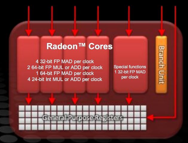
In particular, we can note in figure the structure of the VLIW 5 unit of AMD graphics architectures. The special functions unit can perform one floating point (FP) multiplication and addition (MAD) per cycle, or an execution step of a special function (such as transcendental functions, exponential, etc. ) per cycle.
The remaining 4 execution units can perform 4 32 bits FP MAD, or any combination of addition and multiplication of 2 64-bit FP, one 64-bit FP MAD or any combination of 4 24-bit integer addition and multiplication.
From the comparison with "Redwood", one can see that while the latter has a RAM controller for 128-bit DDR3 or GDDR5 memory, second generation UVD and 4 display controller, even capable of a certain level of Eyefinity technology support, "Sumo" has a direct connection to the 128-bit DDR3 RAM controller on the North Bridge, third-generation UVD and 2 controllers dedicated to the display. If you give up to have the PCI Express x16, you can configure other video outputs, to allow the implementation of the Eyefinity technology.
The integration of on-die GPU and direct connection to the North Bridge has helped the GPU, in part offsetting the fact that you have a DDR3 controller shared with the CPU.
The GPU is indeed connected to the rest of the system by well 3 BUS.
The first link is the "Garlic", which is a direct connection, without coherency check, low latency, 128-bit, between the GPU and RAM controller, arbitrated by the sole RAM controller front-end, which ensures high-priority and low latency. The frequency at which such a link operates would presumably be that of the Northbridge, which should be around 2 GHz, since AMD says it has a bandwidth of more than 30GB/s to the RAM controller, while 2 billion transfers per second is slightly over. It's an improvement over the 64-bit bus for the Ontario/Zacate GPU.
The second link is the "Onion", which interfaces the GPU with the coherent system, composed by the memory, the CPUs and their caches, which is ruled by the MOESI protocol. This direct and low latency connection is a significant step forward. With an external GPU, especially with an IGP, you had to go through the bus connection between the graphics card (or the North Bridge in the case of IGP) and CPU, to wait for its integrated North Bridge controlled the cache and eventually RAM and send the results back. Now the two checks can be done independently and in parallel (through both Onion and Garlic interfaces) and with a much lower latency.
The third connection is the one direct between the GPU and the GIO unit, for access to the PCI Express controller, for an eventual CrossFire with discrete card and video outputs management. The same fate is not up to the cores of the CPU that, to access the GIO, shall pass through the North Bridge and suffer the latencies and waiting.
Another great advantage of an integrated GPU on the same CPU chip is related to the exchange of data in memory. With conventional graphics cards, to render a scene, several data structures must be used: grids of vertices (mesh), color and lighting information and texture mapping for the final color.
These information are created from the 3D software into memory and are passed to the graphics card driver. Because the processes are working with virtual memory, to access them, the driver may even need to load it from disk. In any case they should be transferred to the internal memory of the video card via the PCI Express bus.
Similarly happens for GPGPU calculations, where, in addition, the data must travel even the reverse the route, to load into main memory the calculation results.
All this with an APU is no longer necessary. The Llano APU implements 2 techniques to speed up these operations.
The first is called zero copy, and allows you to not copy the data anymore, but simply to say where they are to the GPU and they may be used directly. This is possible because the GPU can directly access the RAM. But the virtual memory moves data in and out of memory and re allocate it at will. Llano does not yet implement a sophisticated virtual memory manager to help you get an unified memory space. The next architecture will implement it and make the GPU a real vector coprocessor, similarly to first FPU appeared years ago.
To avoid problems, the second technology is employed: Pin in Place. This is to block data structures in a specific area of memory, so the GPU can find and access them safely and they are not to be taken out of memory, on hard disk, extending access times.
When virtual memory will be implemented in future generations of GPU in a manner identical to that of the x86 CPU, then you can talk about unified memory space and such software tricks will no longer be necessary. It would even be possible to page out to disk graphics memory, if they implement the exchange of page fault signals from the GPU to the CPU.
These technologies let, in exceptional cases, have a greater speed than that of a discrete video card. But the sharing of the RAM controller, however, makes the GPU a bit slower than its discrete equivalent.
The GPU, unlike the one implemented in Sandy Bridge, fully supports DirectX 11 and angle independent anisotropic filtering.
Other features supported are OpenGL 4.1, OpenCL 1.1 and MSAA, SSAA and MLAA anti-aliasing techniques.
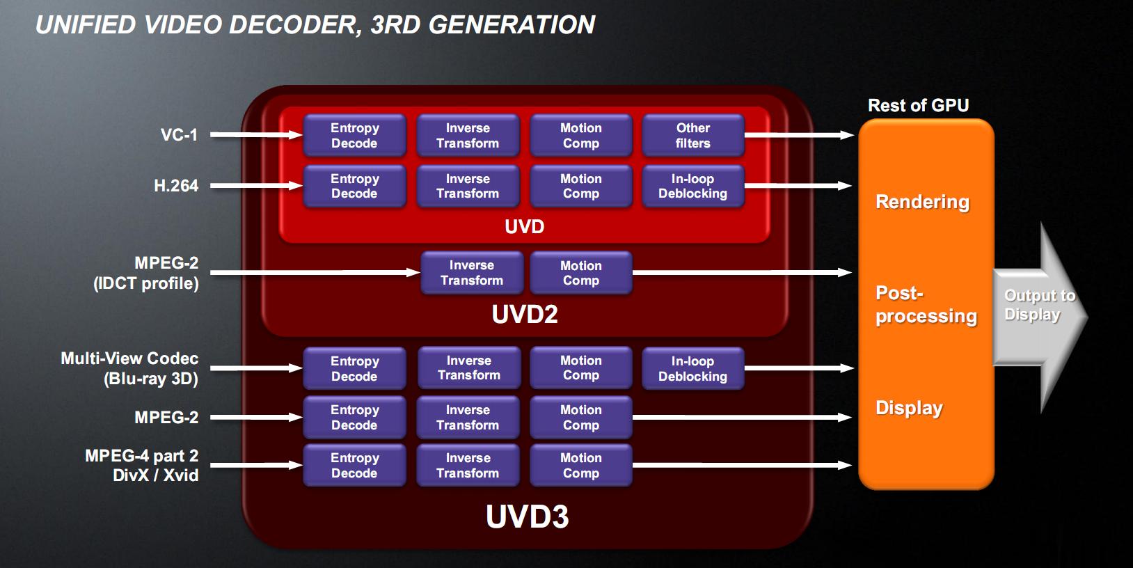
In the picture you can see a block diagram of the various generations of UVD. The third generation, implemented in Llano, can hardware accelerate the MPEG-4 Part 2 (which also includes the DivX and Xvid), MPEG-2 codec and Multi-View Codec (MVC) used to accelerate Blu-ray 3D, which can be viewed through the HDMI 1.4a port which Llano has.
The decoding is all done in the UVD3 block, so the rest of the GPU can be placed in advanced energy-saving (power gating) and save a lot of energy.
Dual Graphics
Last chapter for the GPU is Llano Dual Graphics technology. It allows you to pair, like CrossFire technology, video cards to increase performance. But unlike the latter, it can balance the load between the GPU, taking into account the differences in power.
The mechanism is not perfect, since it is greatly affected by the quality and maturity of the drivers and also works well with DirectX 10 and 11. With DirectX 9, the performance are equal to those of the slower card.
As we saw earlier, CrossFire/DualGraphics and Eyefinity technology are mutually exclusive unless you settle for a smaller number of display interfaces: the x16 PCI Express controller can be divided into two x8 controllers, one of which can be used for CrossFire and one for additional displays. Of course to get the maximum number of video interfaces is necessary to give up to CrossFire support, so as to obtain a full CrossFire support, with x16 interface or two x8 interfaces, to perform a triple CrossFire is necessary to give up to Eyefinity support.
In the event that the performance difference between the discrete card or cards combined with the GPU will be high, the performance increase over discrete card usage only is fairly modest.
In compensation, however, AMD has implemented the drivers so you can route OpenCL 1.1 calls to the integrated GPU without impairing the discrete GPUs, if they are working on a heavy 3D load.
AMD Turbo Core 2.0 and AMD System Monitor
TurboCore technology evolves from its first implementation in Thuban. In this architecture, the clock increase was made only in very specific conditions, ie when 50% of the cores were idle, and only with an on/off logic, regardless of the TDP margin.
This is because the first implementation of TurboCore was very conservative, since it did not verify in real time the actual consumption. So the conditions for intervention and the margin of clock increase had to be kept very conservative to avoid exceeding the TDP even in the worst case.
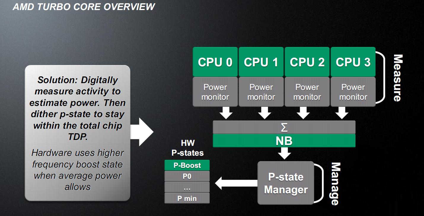
This all changed with the TurboCore, version 2.0. First, it was introduced an unit called APM (Advanced Power Management), which digitally measures 95 signals for each core, plus others scattered throughout the chip, to estimate, with an accuracy above 98% (ie less than 2% of error margin) the power dissipated in a range of one hundredth of a second, or 10 ms.
Comparing this situation with that of Thuban, where the overclocking intervention was carried out in a modality so-called open-loop, ie where the effect of the increased clock on the TDP is not brought back and then you must be very conservative, the TurboCore 2.0 intervention mode can be classified as a closed-loop (with feedback), since it measures the actual TDP and is able to implement an adjustment.
The APM measures an estimate of the TDP by not taking into account the temperature and in a fully digital mode: essentially measures the percentage of activities of various units, obtaining the total consumption, knowing the maximum of each unit.
Confronted with the measuring method of the Intel counterpart, analog and strongly temperature dependent, we have a very reproducible pattern of the clock for Llano, although potentially not optimal because the maximum TDP could not be reached, because of safety margins, though present, for overclocking.
Another novelty is the clock increment mode of TurboCore. While in Thuban was of on/off type, in Llano uses a dithering algorithm, which is to calculate the percentage of time, of a preset time interval, the CPU should be clocked higher than the base state, so that the average power during the interval is as high as possible, while remaining below the TDP. This also implies that the "effective" frequency of the CPU is an intermediate value between the default value and the Turbo value. That is, the CPU behaves as if it runs at the intermediate frequency. Let's take an example with top of the range Thuban frequencies. The base frequency is 3.3GHz and the turbo frequency is 3.7GHz. Suppose that the maximum TDP is 100W, as for Llano. Suppose, finally, to have a workload that make the CPU absorb 90W at 3.3GHz, but 102W at 3.7GHz. If we implement the increase in the clock as Thuban, even with the APM, we can not increase the clock, because we know that we could not stay within the TDP. This algorithm calculates the optimal percentage of time that the CPU must be in the upper clock state. Suppose that the calculation says that with 90% of time in the turbo state, the TDP is 99W. Just below the limit. The effective frequency of the CPU is 3.3*0.1+3.7*0.9=3.66GHz. This is a great advantage over Thuban architecture and also over Intel architecture: in this case, the number of turbo states is limited and you must go in increments of 100 or 133MHz. With the mechanism of AMD, however, you can virtually have the whole range of effective frequencies ranging from the base, in which is guaranteed to not exceed the TDP, and the upper clock.
This allows you to maximize the capabilities of the dissipative system and allows you to select a higher frequency of Turbo: Thuban was in fact limited by the fact that it could change the CPU clock speed with a certain speed without being able to modulate, with a dithering algorithm, the time spent in the high clock state.
As for the Thuban, the higher clock P-state is an hardware state invisible to the operating system, which detects that the CPU is always in the state of maximum speed, but the default frequency.
This causes problems in the revelation of the actual frequency of the CPU and in fact there have been added some internal registers (the family of so-called MSR Model Specific Registers, read with the CPUID instruction), which allow you to calculate an average effective clock of the cores, because they automatically count the number of clock ticks seen by the CPU in a given interval.
In Llano only the CPU can increase its clock, even though AMD has reserved the possibility to also increase the GPU clock in future models (and it would seem that already the successor of Llano, Trinity, based on Bulldozer architecture on the CPU side, can implement it).
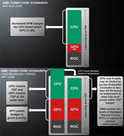
Until now, we have seen that the temperature of the chip has not actually entered into the turbo equation. But there is a protective mechanism that lowers the CPU clock below the default value if the temperature exceeds the critical values.
Apart from the failure of the cooling system, the only way that this can happen is compute-intensive scenarios, where both CPU and GPU are committed to the maximum. These programs can be specifically developed for stress testing or even OpenCL programs that engage to the maximum the CPU and the GPU.
AMD System Monitor
AMD has developed a monitoring software particularly suited for the new Bobcat and Llano APU, which also works with older systems, detecting and monitoring AMD components (CPU, GPU, APU and IGP) in the system.
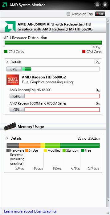
The application has two levels of detail that can be selected independently for the computing elements (CPU, GPU, IGP, and APU) and the memory, via the button marked by the word Details.
At the lowest level of detail in the section relating to the CPU, the application shows the usage as a percentage for the single cores. If there is an APU is also shown the division of resources between core and GPU.
In the GPU section the percentage of utilization of installed AMD GPUs (including discrete cards, IGP and graphics of the APU, manufactured by AMD) is displayed.
In the memory section the distribution of memory between the various types in the system (reserved in hardware, in use, modified, in standby) and free memory, expressed as a percentage of total memory, is displayed.
At the higher level of detail in the section relating to the CPU, additional detailed information are shown for each core, including the approximate operating frequencies.
In the GPU, in addition to basic information, the frequencies of the GPU and video memory and the current speed of the GPU fan (if present) are displayed.
In the memory section, in addition to basic information, additional details of the system, including the frequency of main RAM memory are displayed.
Conclusions and future trends
The Llano architecture is much more that a merge of a Propus class CPU and a Redwood class GPU.
There was implemented various energy saving techniques and hardware and software infrastructure capable of exploiting the possible synergies when two components are integrated on the same chip.
The performance/consumption ratio at platform level is increased both compared to previous AMD platforms, both with respect to the competitor platform, especially considering the applications which make use of GPU acceleration.
The chip real estate is a compromise in favor of the graphics in the AMD architecture, where it can boast more experience and know-how derived from the acquisition of ATI.
Besides, the future trend, thanks to the promotion of GPGPU, results in a greater use of graphics processor for non strictly recreational tasks.
The main reason is the vast computing power of the GPU, coupled with a quite acceptable consumption, which makes the performance/consumption particularly favorable.
This does not mean that the CPU will be abandoned, because there are tasks in which they are more efficient than GPU.
Driven integration between these two elements is desirable and the future in this direction: the Bulldozer architecture releases more emphatically the FPU from the rest of the core, setting the stage for possible future use of GPUs as a math coprocessor.
The missing piece is the unification of the address space between CPU and GPU, which is implemented in Llano at the driver level, but with subsequent architectures should be implemented at an even lower level.
Once these features were implemented, the term Fusion will take the essence of the AMD strategy.
Marco Comerci
CPU tests performed by Angelo Ciardiello