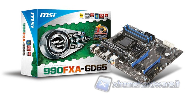
 MSI 990FXA-GD65 is proposed as high-end motherboard for AMD AM3+ CPU, so compatible with the upcoming AMD Bulldozer. Powered by the AMD 990FX chipset, it has nice features, that we will discuss during this review.
Pubblicità
Packaging and First Contact
Let us see now more closely the 990FXA-GD65 of the well-known manufacturer MSI, one of the most promising motherboard both in technology and for quality construction.
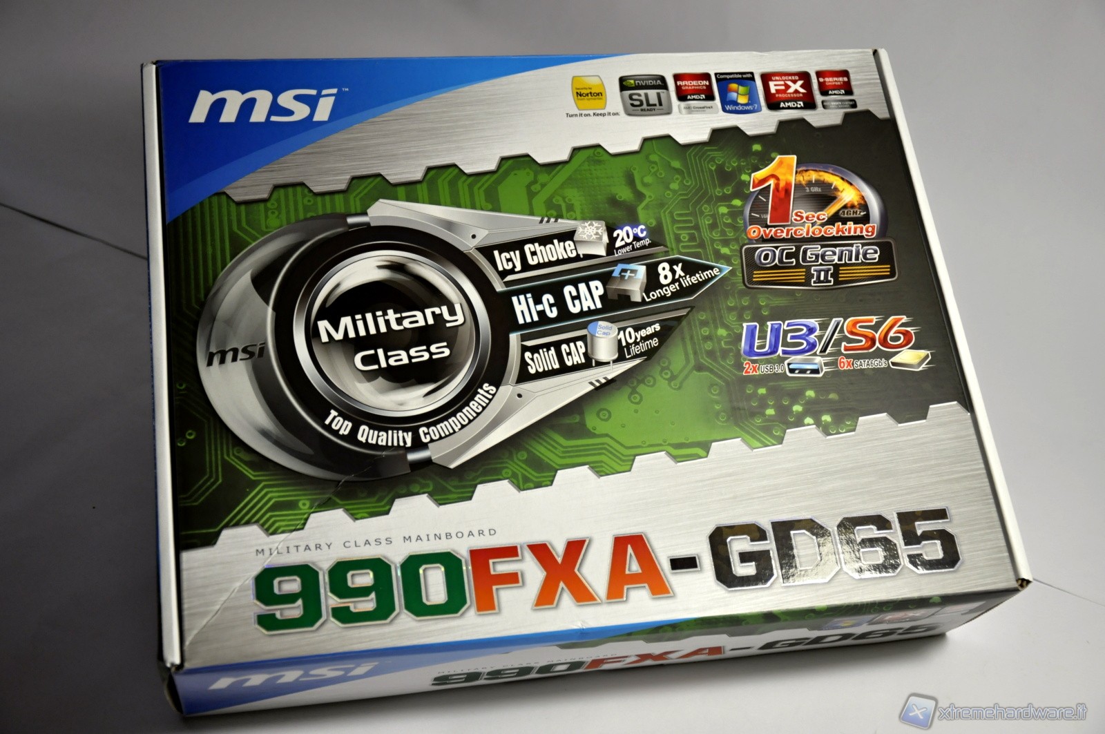
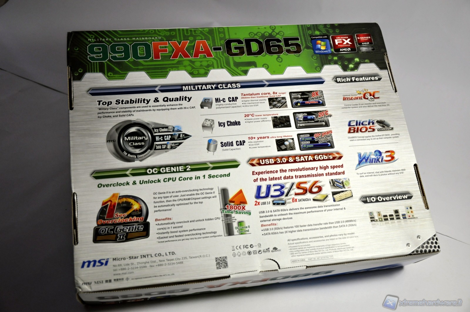
The package comes with some very bright colors. Front from the top we have the name of the company that produces it, MSI, and a series of icons representing the technologies offered that we mentioned in the previous section. At the center part of the proprietary technologies adopted by MSI products in the Military Class series and at the bottom there is the model of the board. At the back of the pack there is a more than a summary explanation of the features given early on the front and that we talked about in the previous section.
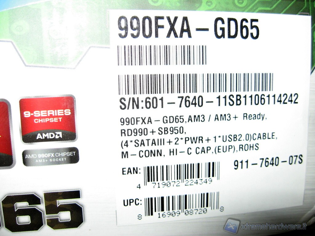
In the label in the picture, we get some summarized information that characterize this product, in addition to the model and serial number.
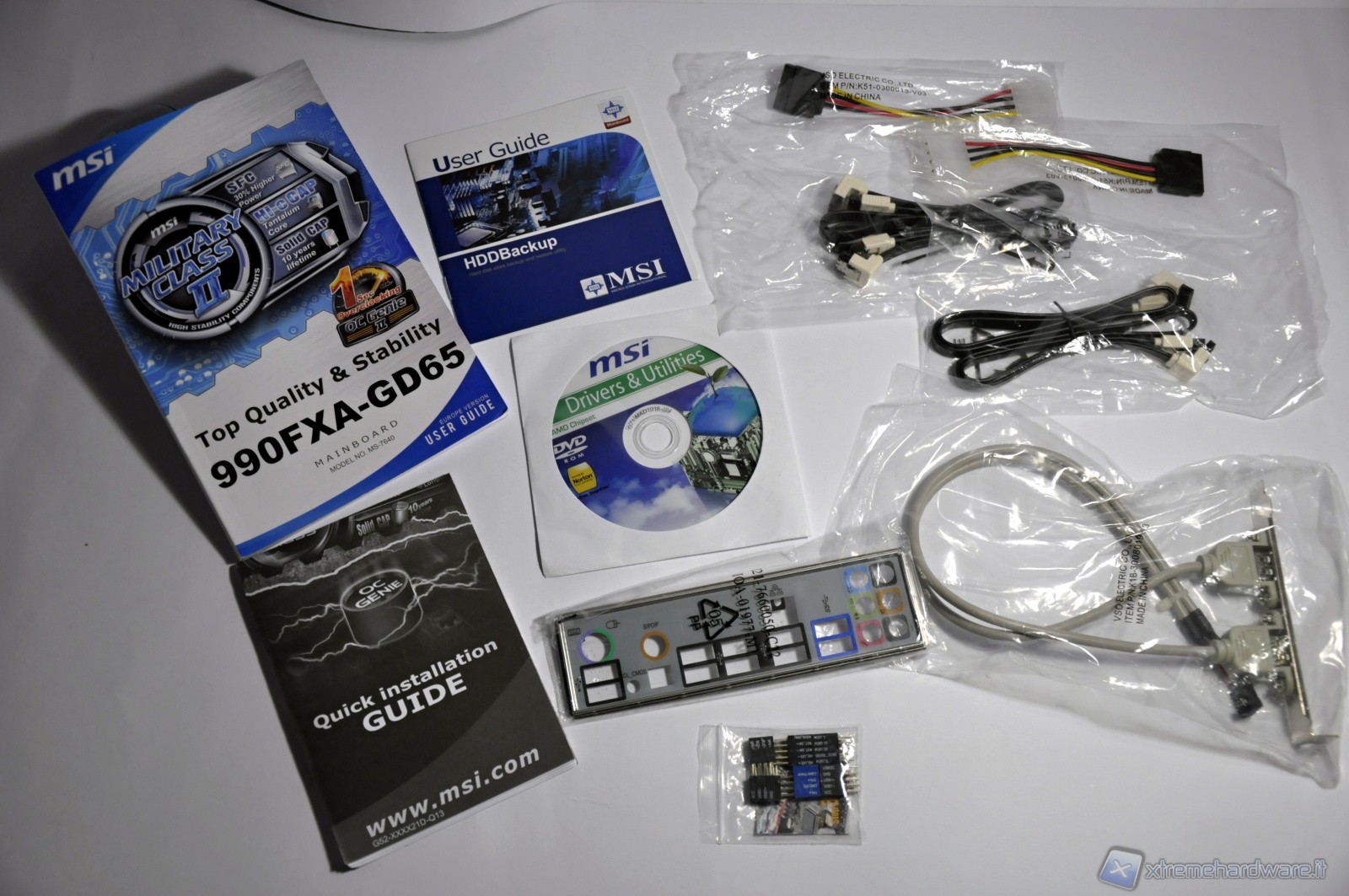
The material accompanying the MSI 990FXA-GD65 is as follows:
- Multilingual Manual including Italian, unfortunately, very brief
- Additional brochures for quick installation
- A user's guide for backing up on hard drives
- CD-ROM containing drivers, utilities and Norton Antivirus
- I/O mask for the board assembly in the chassis
- Various sockets for fast wiring of various wires from the chassis
- 2 molex (4 pin) to SATA power connector adapters
- 4 6Gbit/s SATA cables
- Bracket for mounting on the chassis 2 USB ports
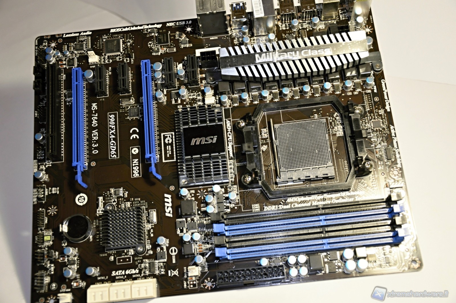
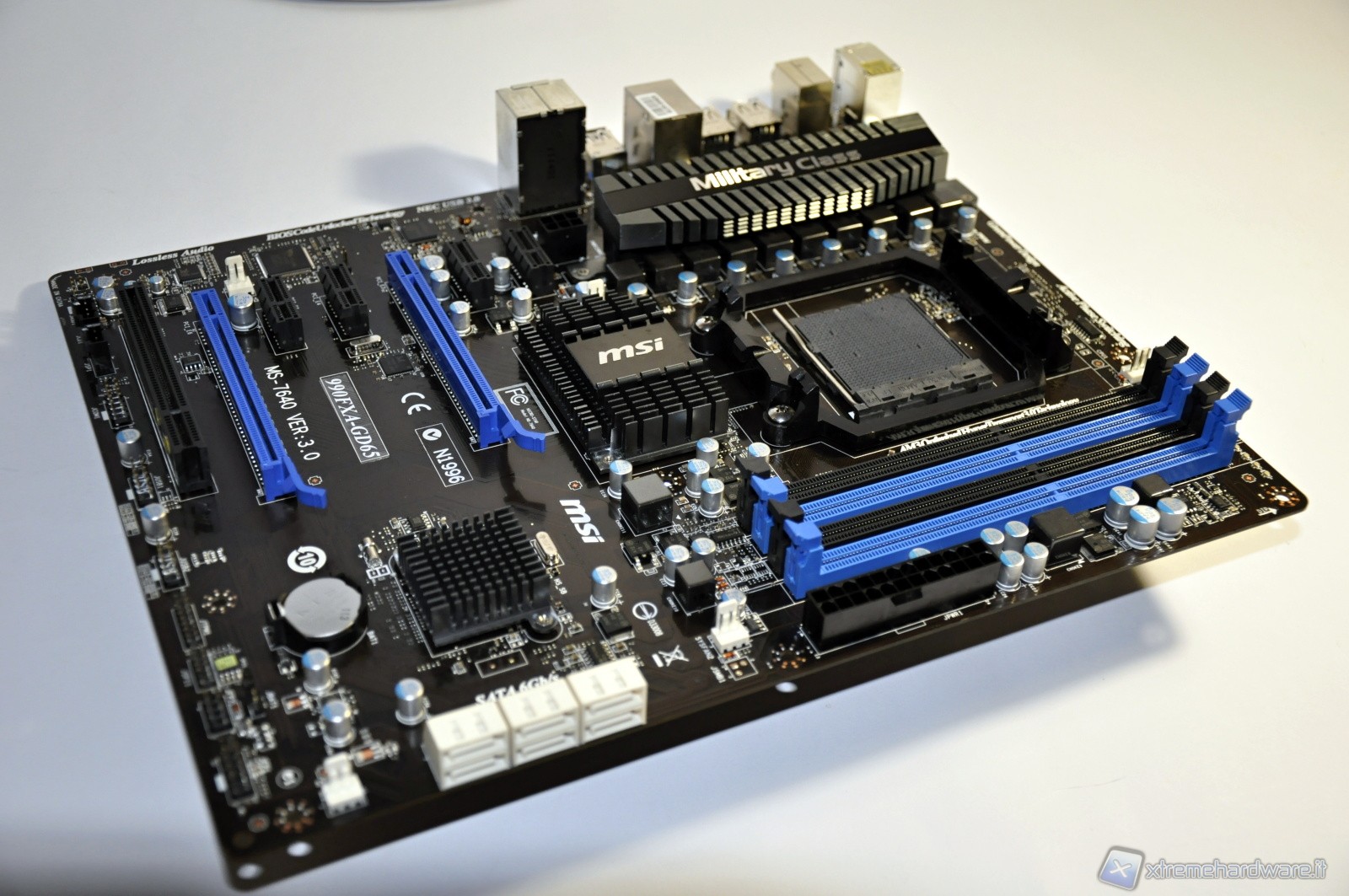
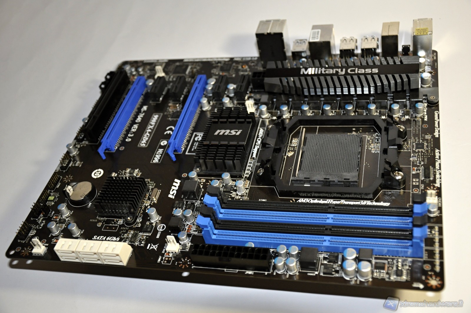
The layout seems well-ordered with lots of free space around the socket, especially if you remove the bracket pre-installed to allow the mounting of liquid/nitrogen heat sinks (for high-end overclocking). This will be very pleased to overclockers. In the picture you can see the black bracket for attaching the standard heat sink. To disassemble just unscrew the 4 screws that hold it together with the metal plate below.
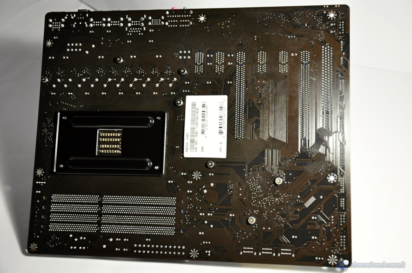
Here are the pictures of the underside. As you can see the surface is clean with no significant findings, except for the socket retention bracket, which is not glued but fixed with screws. This facilitates and simplifies the neoprene insulation operations when you want to run high-end overclock tests, using nitrogen.
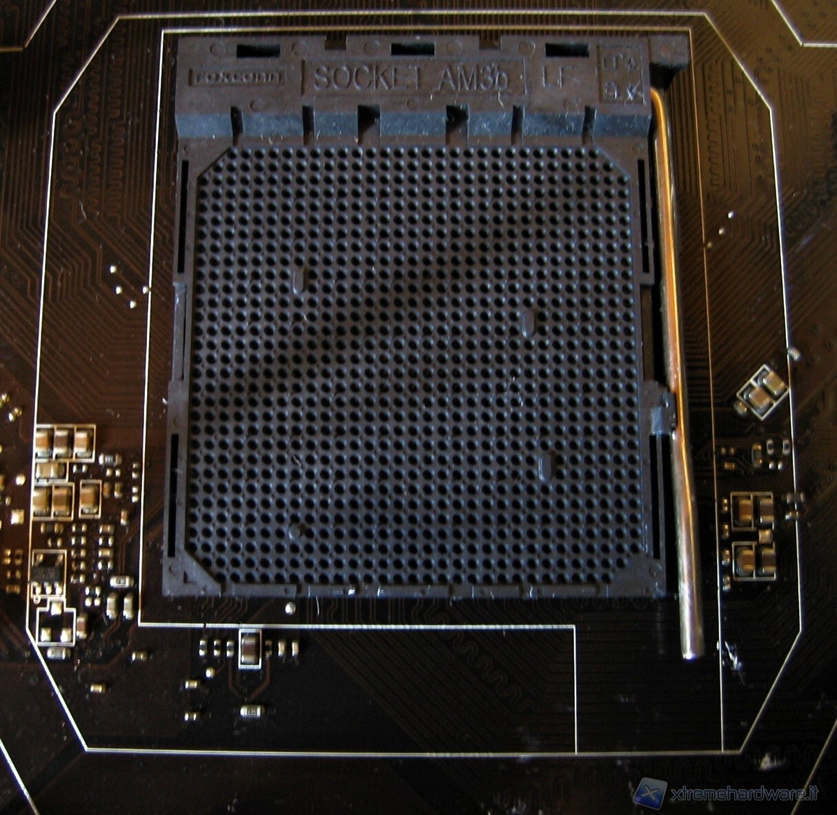
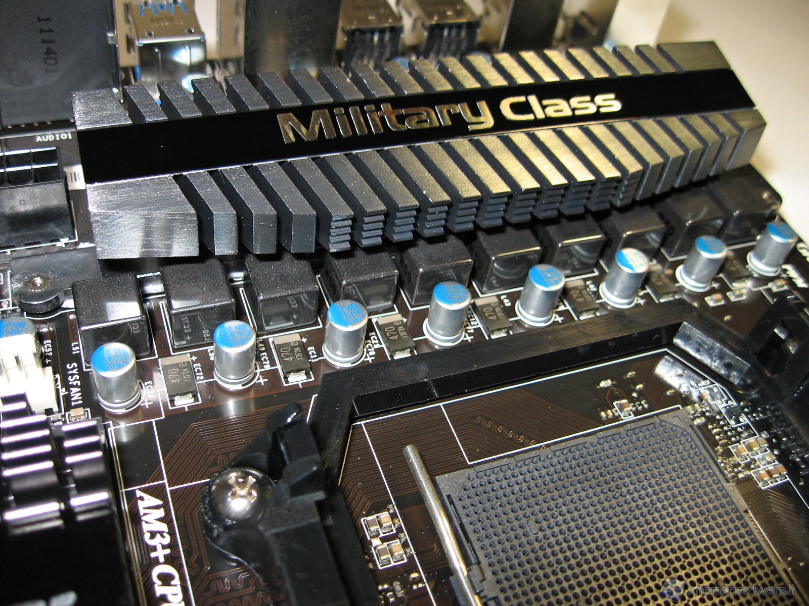
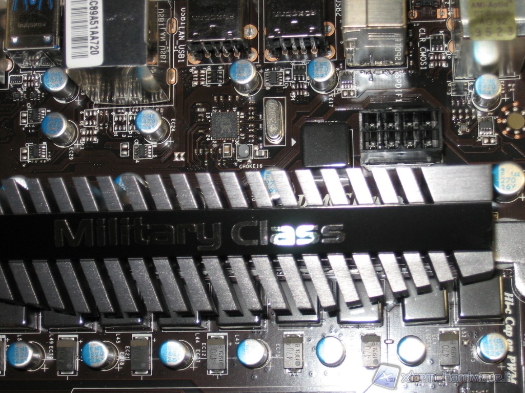
The AM3+ socket (or also called AM3b), unlike the Intel is a socket with many holes, exactly 942, where they are going to fit CPU pins. Logically it has its orientation, so be careful when installing. Next to the socket we note the 10 power phases with Military Class components. First we have the Hi-C Cap with the traditional solid Cap. In the second row we see the Icy Choke chokes, while under the big heat sink are the mosfets.
If you want to cool the processor through a liquid cooling system, then water block, the movement of air from the fan installed on the CPU cooler air would be lost. It is advisable to consider the installation of a fan nearby to cool this area.
To ensure the full stability, we're going to check, and delivery sufficiently adequate amperage required by the current 45nm and future 32nm CPU, we can highlight in the photo on the right the black 8-pin connector attack for the additional processor power.
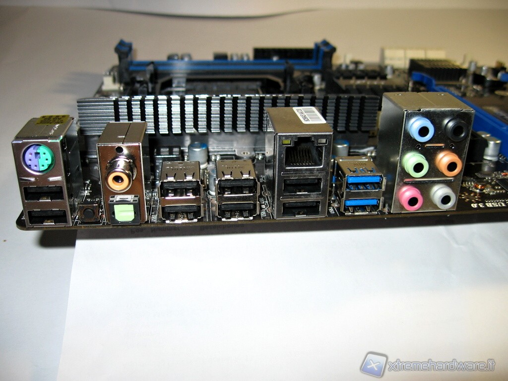
Starting from the left in this photo we have the mixed PS2 attack for the keyboard or the mouse and below the first 2 USB 2.0 ports. Further we have the button to immediately reset the CMOS memory. Continuing on the right we have from above the connection for coaxial SPDIF output and below the optical SPDIF output. On the right we have 2 blocks of 2 USB 2.0 ports. Following that we find an Ethernet port (in Gigabit standard) and other 2 USB 2.0 ports. Then in blue to differentiate them from other, 2 USB 3.0 ports, and finally the block dedicated to the connectors for the input and output of the audio channels.
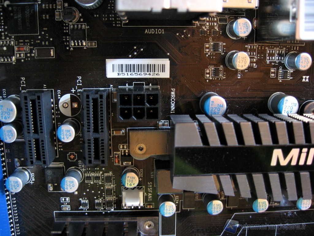
Leaving the sockets/ports area, going to the left we see the 6-pin connector for additional power supply of the PCI-Express and then of the graphics card. Note the wording NEC USB 3.0 and the D720200AF1 chip. We remind readers that in the introduction we said that both AMD and Intel have not implemented natively this standard (except for Llano), but rely on external chips.
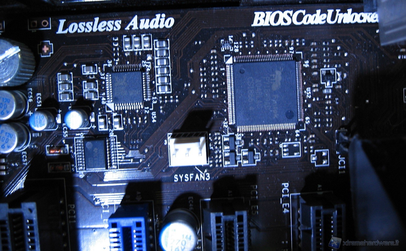
Here is the macro shot of the Realtek ALC892 chip (left) dedicated to the signal. You can find additional details at this address: Realtek ALC892 .
On the right we see the Fintek F71889AD chip dedicated to hardware monitoring of voltages and temperatures as well as to assist the OC Genie II tool.
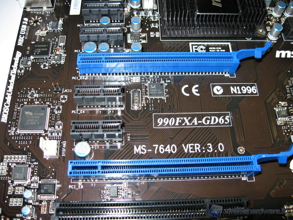
In this photo we see the area of the slots that house the internal cards. In black the 1 st, 2 nd, the 4 th and 5 th are PCI-Express x1. In blue the 3 rd and 6 th are PCI-Express x16 full length for graphics cards or scaling to lower speeds such as RAID controllers for PCI-E x8/x4. The slot can operate simultaneously at full bandwidth (x16, x16). The 7 th black slot, not to be confused with other shorter is 32bit PCI type and can accommodate cards compatible with this standard. On the PCB of the card printed in white letters we see the model/version of the MSI 990FXA-GD65 we are reviewing.
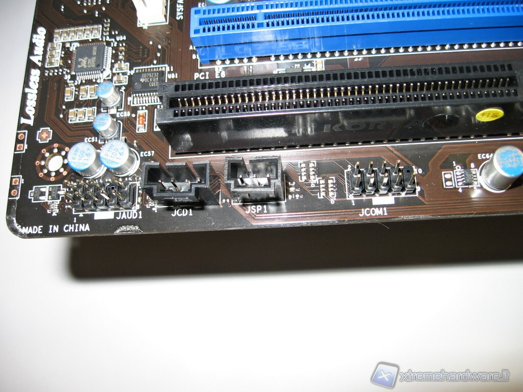
We now move to deepen the area reserved for connectivity and so to the connecting of all those cables that replicate on the chassis (front and back) the various ports. From the left we have a dedicated connector to the Front Panel Audio, i.e. to replicate the input/output of the ports/speakers from the chassis. With the words in white JCD1 we have the internal connector for the audio signal output. The JSP1 connector is the one dedicated to duplicate on the case the S/PDIF output. Immediately to the right then JCOM1 is dedicated to the serial COM port output.
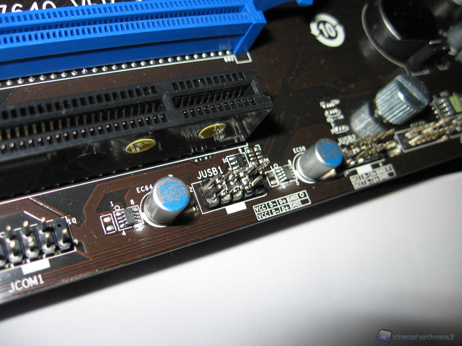
Still on the right with JUSB1 and JUSB2 we have other 8 USB 2.0 ports. An attack will host the bracket shown in the bundle.
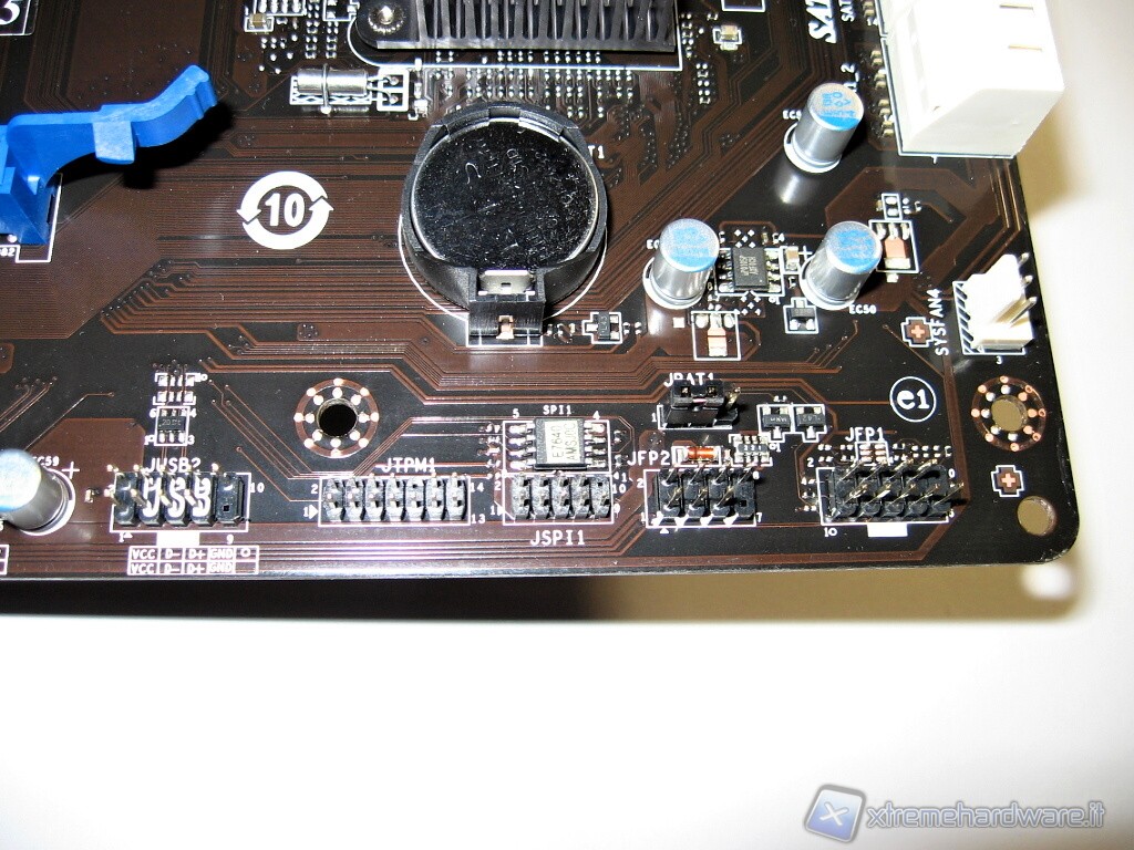
The JTPM1 area is devoted to a possible optional TPM module (Trusted Platform Module). On JFP1 and JFP2 we will connect all the cables from the main front panel of the case, namely the Start button, Reset, activity LED of the hard disk and the speaker. Above we see the classic button-type battery for storing settings/timer in the CMOS and at its right the JBAT1 3 pin jumper to clear the CMOS.
Changing the side or following along the perimeter of the PCB we have a 3-pin connector to power the chassis fan.
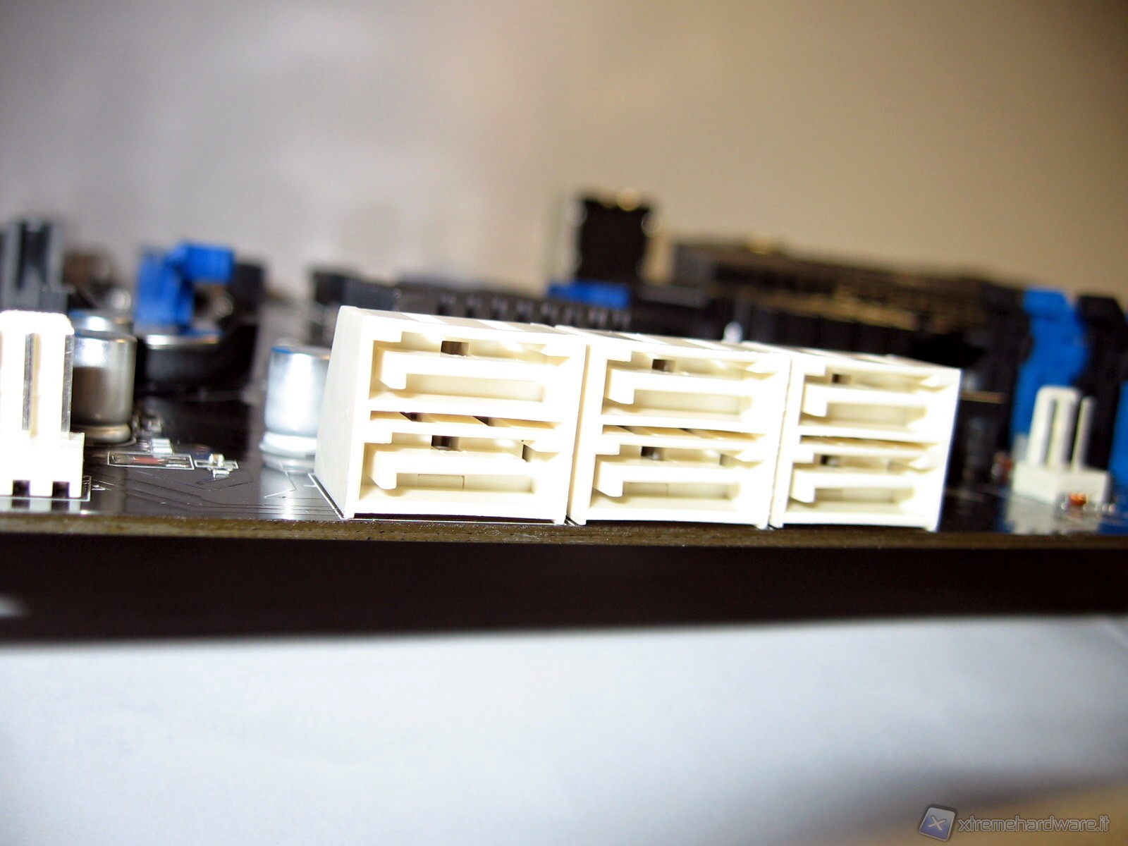
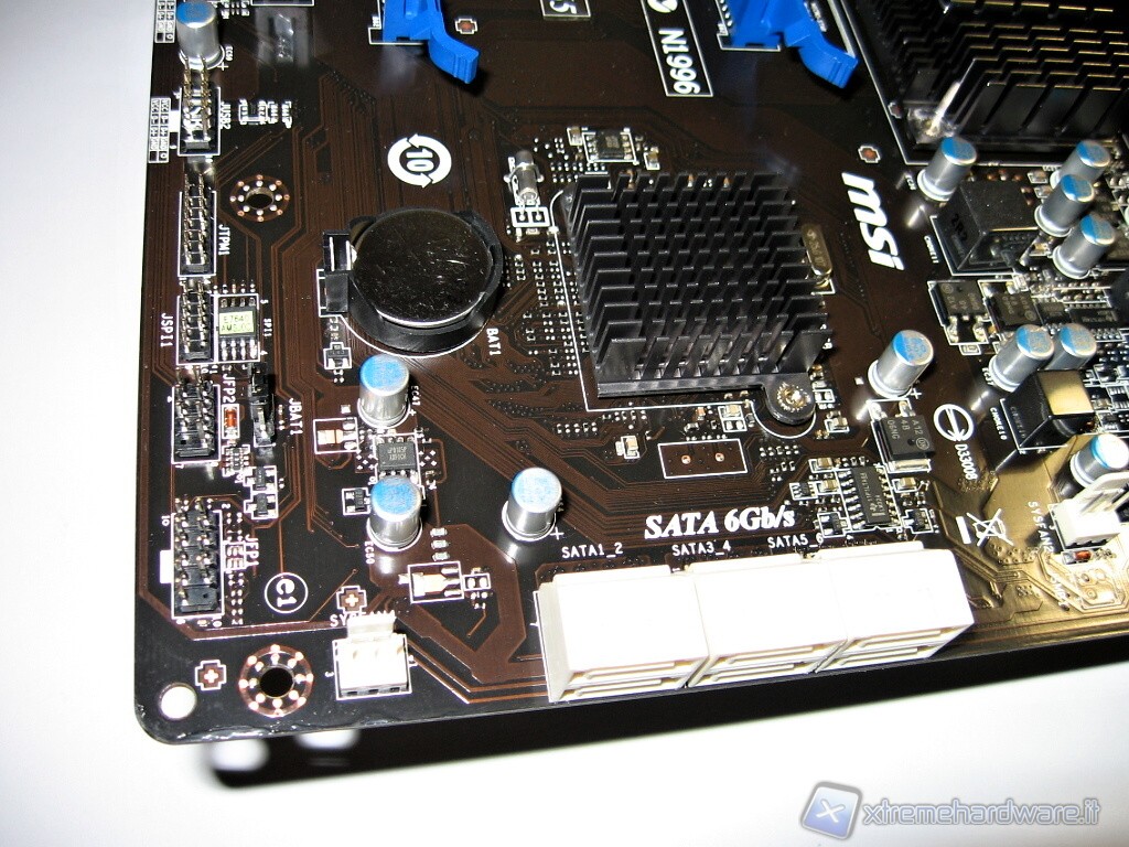
To its right we have the 6 6Gb/s SATA ports and yet another attack on the right always another 3 pin fan.
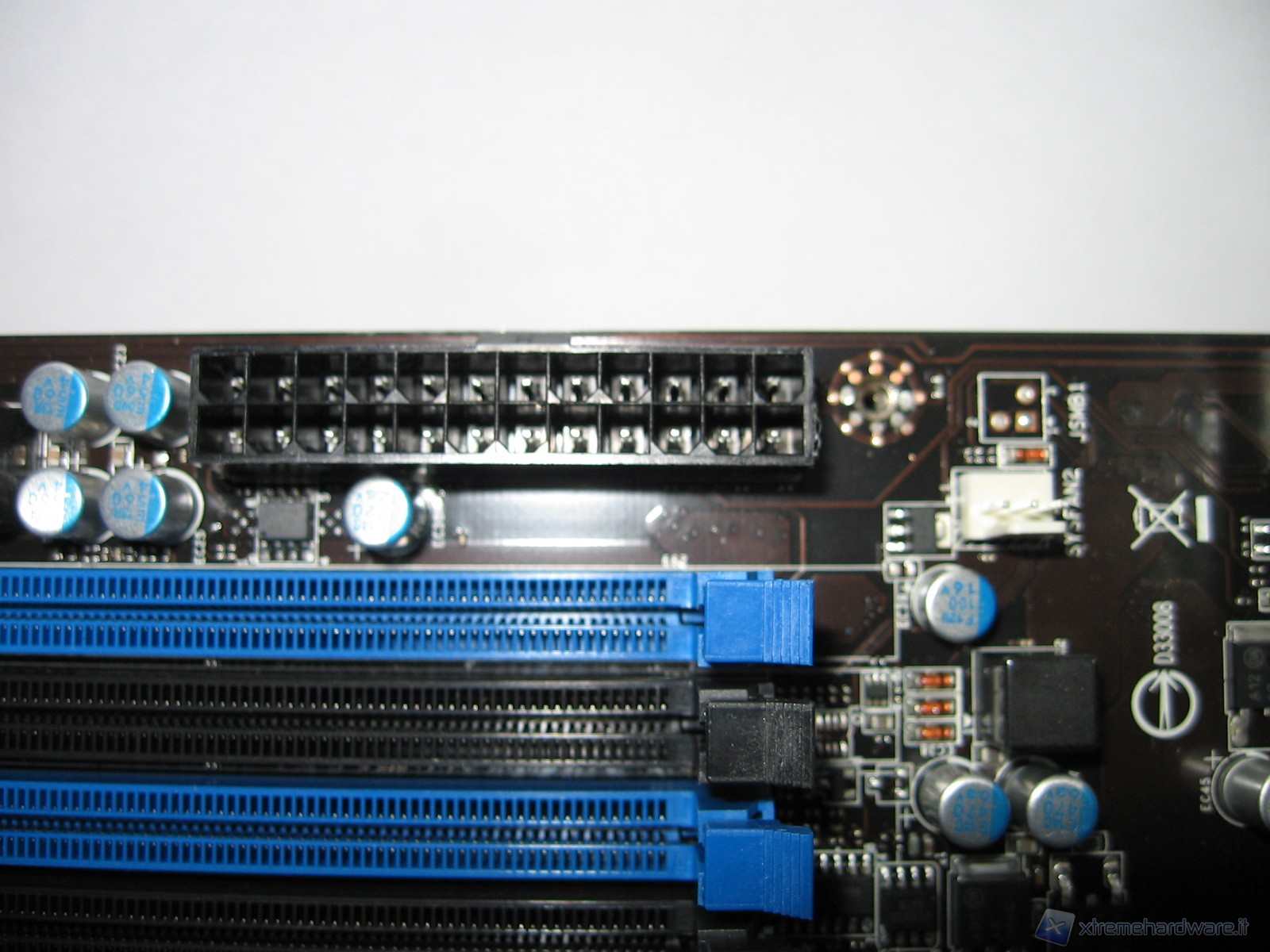
In the picture the classic 24-pin ATX v2.2 Power connector for the main power supply to the motherboard.
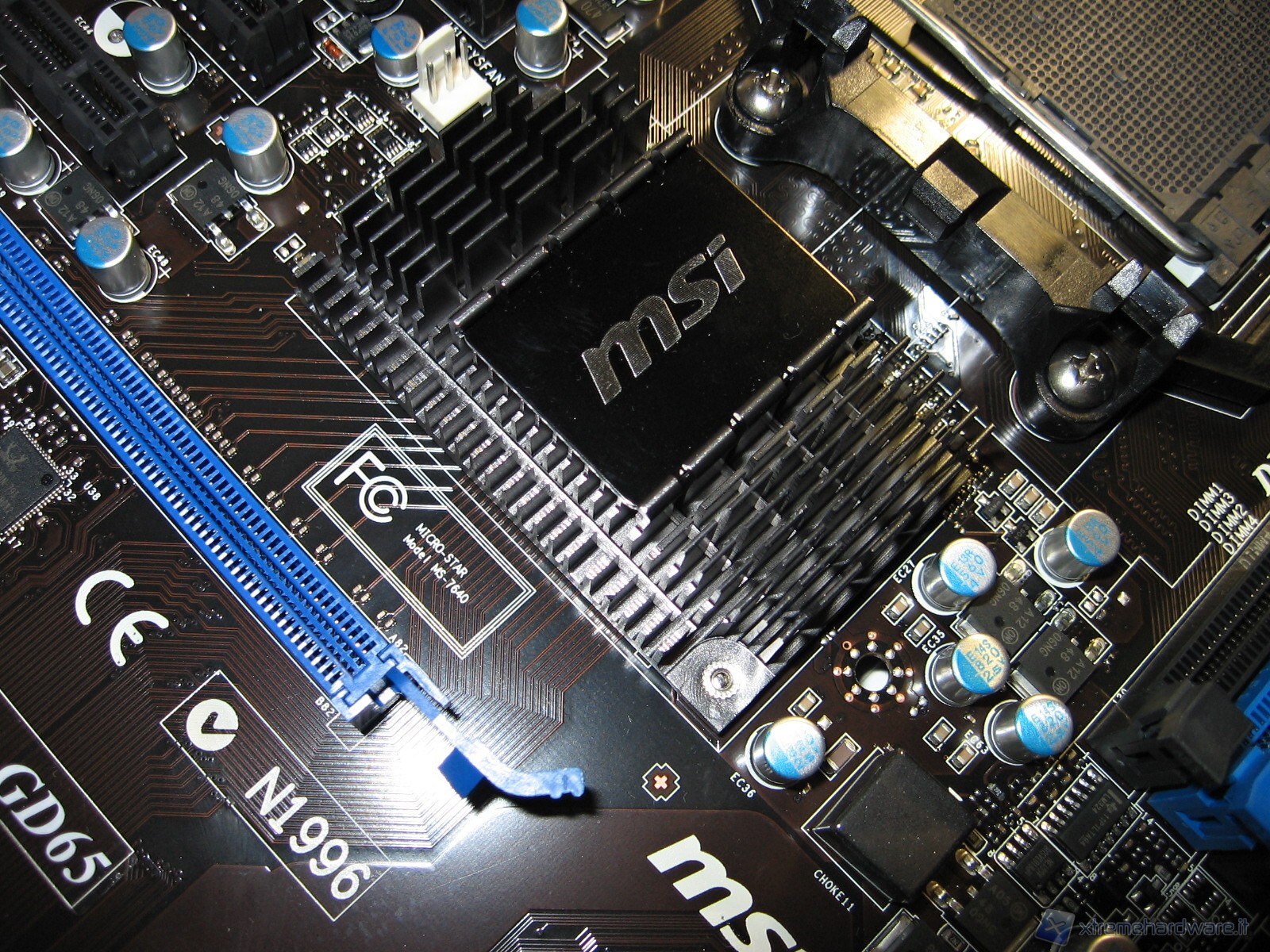
On the other hand we can see the photos of the Northbridge passive heat sink. Here, too, same thing as the heat sink of the socket area, it is good that there is in the vicinity a fan who dispose of the heat produced, especially in the presence of future 8 cores Bulldozer CPU.
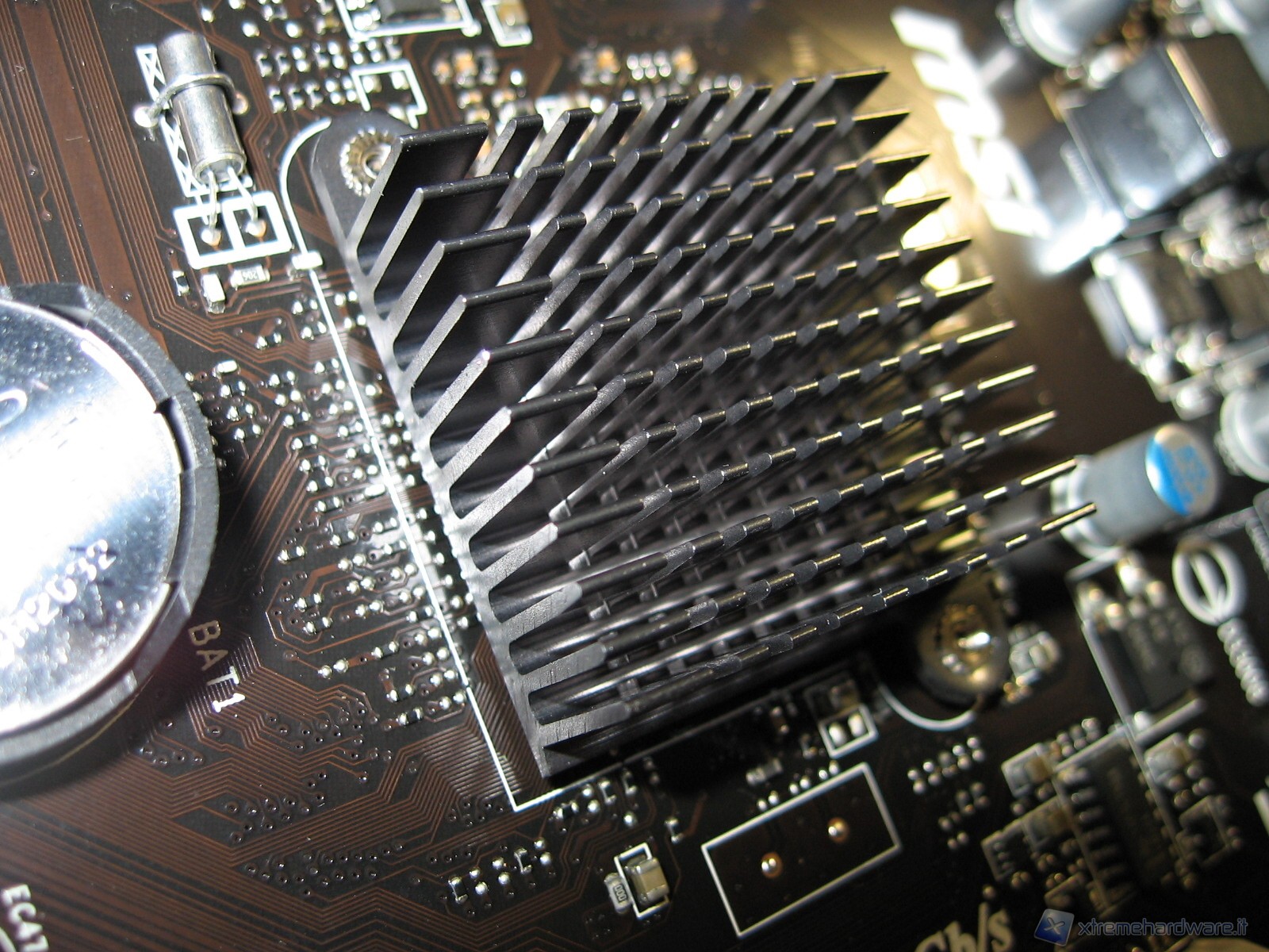
Under this passive heat sink is the SB950 Southbridge chip.
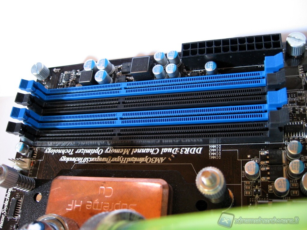
Framed in pairs of 2, the 4 blacks and blue slots dedicated to the DDR3 memory modules, with overclocked speeds up to 2133MHz.
Let us now examine together the BIOS.