AMD Fusion and A-Series APU
The concept of AMD Fusion should now be clear. The purpose of AMD is to "merge" the CPU, GPU and Northbridge in a single chip to reduce energy consumption and production costs while striving to maximize performance for a rather broad target range of users.
This target focuses on displaying information in graphical form, representing the future of the IT world. AMD is committed to providing unparalleled performance in this area, allowing users to benefit from a versatile platform and to meet a wide range of uses.
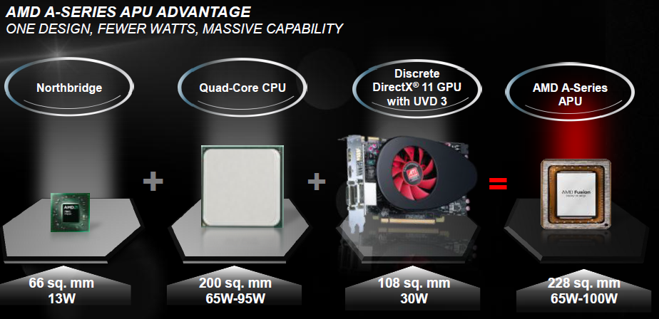
The slide that illustrates the process of "fusion" leaves us no doubt stunned. AMD has integrated one 66 mm2 chip (the Northbridge), one of 200 mm2 (the quad core CPU) and one of 108 mm2 (a DX11 GPU with 400 processor Stream) in an area of only 228 mm2 of silicon.AMD Alchemy continues in terms of energy balance and TDP, where the Llano APU keep the TDP of the previous quad-core CPU generation, despite the integration of graphics processing units.
Since mathematics is not an opinion we try to explain the AMD Fusion "miracle".First, the main factor that has reduced the occupied silicon area, as well as consumption, is the introduction of the 32nm SOI manufacturing process. It's an important step for AMD that finally manages to fill the technology gap against Intel.
The benefits of switching to new production process are evident. Until now, desktop and mobile AMD CPUs were using the 45nm process, while the GPU were using a 40nm process. Integrating all on a 32nm chip helps us understand the truthfulness of the sum presented in the AMD slide. The efficiency improvements are significant also in relation to the previous E series Zacate and Ontario APU, which adopt a 40nm manufacturing process, derived directly from the GPU. In addition, the cores have been completely redesigned with the goal of energy saving by turning off unused portions at any time, optimizing the layout of the clock circuits and implementing various deep off states of cores. All of this extended to other parts of the chip, as the GPU, northbridge and UVD unit.
Obviously there's more. Comparing an Llano APU to a quad-core Intel Sandy Bridge we can not do nothing but notice the lack of L3 cache, the supporting heart of the Sandy Bridge architecture. AMD has chosen to increase up to 1MB the L2 cache compared with only 256KB of Intel's.Instead there is no shared cache between cores and IGP. The elimination of L3 cache leads to a significant savings in area and the ability to deploy advanced energy-saving states, that with the unique architecture of the AMD cache, would have been costly and inefficient to implement, for the benefit of graphics processing units.
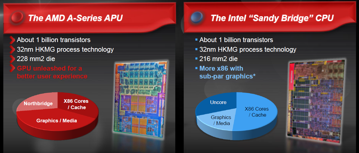
Analyzing the percentage by which they divided the two CPUs (APU and SB) we can clearly see how much silicon has been reserved in the APU for the graphics unit of AMD. Almost twice as used by Intel, coming to occupy almost one third of the entire die.In the picture we see distinctly 5 SIMD engine at the top of the die, while below are the 4 x86 core with its L2 cache.
The 5 SIMD engine have 80 stream processors each, for a total of 400 stream processors. It's a very large number, superior even to the Caicos GPU that equips the HD 6450, entry level in the desktop market. It's in fact very close to the stream processors number composing an HD 6570 or HD 6670 that integrates 6 instead of 5 SIMD engines present in Llano APU.
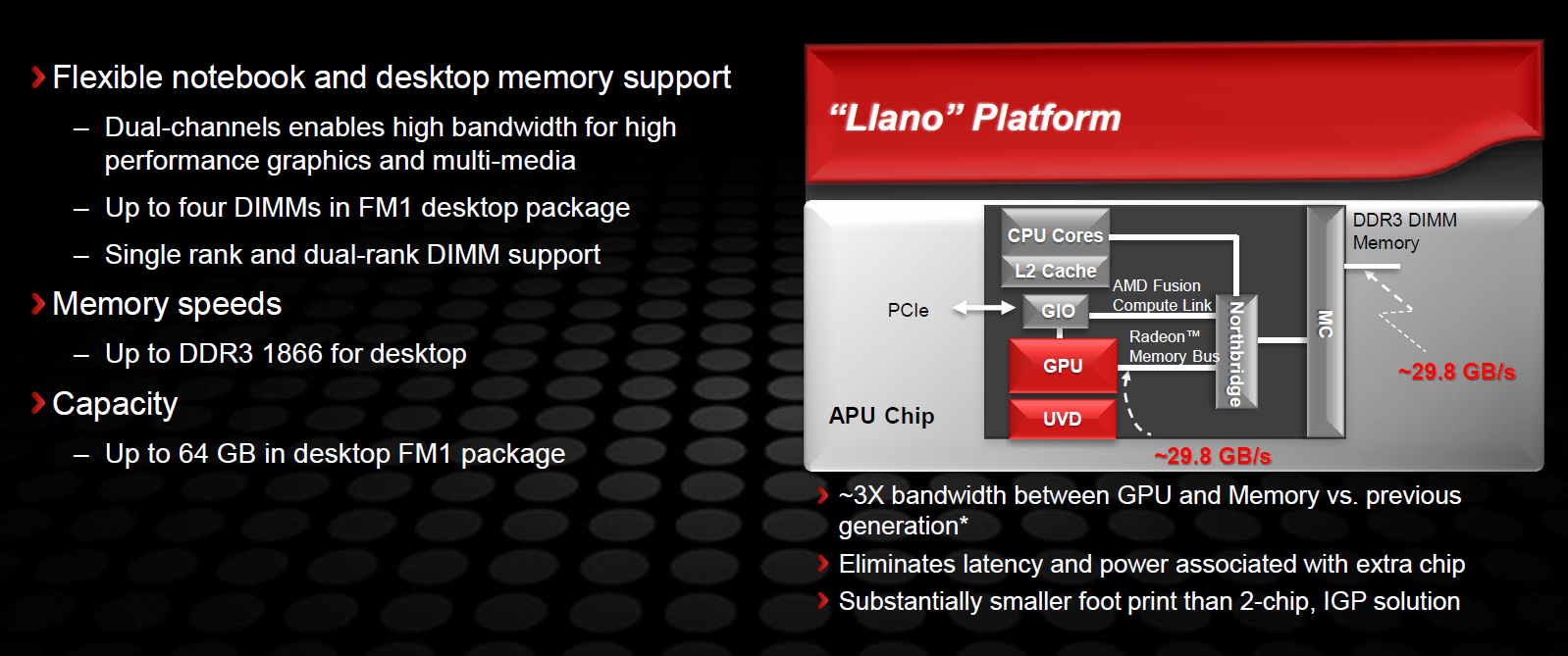
Obviously, the IGP has at least one disadvantage over a discrete video card: the lack of dedicated memory. The graphics core of the Llano APU must in fact go to the system RAM, the same which needs to access the CPU. This involves slow access compared to an onboard memory, especially given the lack of an L3 cache that can serve as a common buffer. AMD has tried to balance this disadvantage trying to support memory at higher frequencies than for example the Zacate APU, raising the supported clock up to DDR3-1866.
But one interesting feature of the Llano APU is the Dual Graphics, a CrossFire technology improvement, which takes into account the relative power of the GPUs. In addition, the drivers are optimized for the OpenCL, using the integrated GPU for the less burdensome calculations if the discrete one is processing heavy 3D loads. As an alternative to DualGraphics, the PCI Express link can be configured as additional video outputs to implement the Eyefinity technology in a more advanced configuration.